Rainbow Electronics MAX547 User Manual
Page 6

MAX547
Octal, 13-Bit Voltage-Output
DAC with Parallel Interface
6
_______________________________________________________________________________________
PLCC
NAME
1
–
C
—
L
—
R
–
Clear Input (active low). Driving this asynchronous input low sets the content of all latches to
1000hex. All DAC outputs are reset to AGND_.
3
REFCD
Reference Voltage Input for DAC C and DAC D. Bypass to AGNDCD with a 0.1µF to 1µF capacitor.
2
AGNDCD
Analog Ground for DAC C and DAC D
7
VOUTB
DAC B Output Voltage
6
VOUTC
DAC C Output Voltage
5
VOUTD
DAC D Output Voltage
4, 42
V
SS
Negative Power Supply, -5V (2 pins). Connect both pins to the supply voltage. Bypass each pin
to the system analog ground with a 0.1µF to 1µF capacitor.
FLAT
PACK
PIN
39
41
40
1
44
43
42, 36
FUNCTION
8
VOUTA
DAC A Output Voltage
2
9, 37
V
DD
Positive Power Supply, 5V (2 pins). Connect both pins to the supply voltage. Bypass each pin to
the system analog ground with a 0.1µF to 1µF capacitor.
3, 31
10
REFAB
Reference Voltage Input for DAC A and DAC B. Bypass to AGNDAB with a 0.1µF to 1µF capacitor.
4
11
AGNDAB
Analog Ground for DAC A and DAC B
5
12
–
L
—
D
—
A
—
B
–
Load Input (active low). Driving this asynchronous input low transfers the contents of input latches
A and B to the respective DAC latches.
6
13
–
L
—
D
—
C
—
D
–
Load Input (active low). Driving this asynchronous input low transfers the contents of input latches
C and D to the respective DAC latches.
7
14
–
C
—
S
–
Chip Select (active low)
8
15
–
W
—
R
–
Write Input (active low).
–
W
—
R
–
, along with
–
C
—
S
–
, loads data into the DAC input latch selected by A0–A2.
9
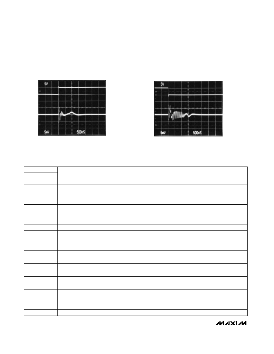
ADJACENT-CHANNEL CROSSTALK
A: DIGITAL INPUTS, DAC A, DATA BITS from ALL Os to OAAAhex
B: OUTPUT, DAC B
500ns/div
REF– = 4.096V, C
L
= 50pF, R
L
= 10k
Ω
A
5V/div
B
5mV/div
ADJACENT-CHANNEL CROSSTALK
A: DIGITAL INPUTS, DAC A, DATA BITS from OAAAhex to ALL Os
B: OUTPUT, DAC B
500ns/div
REF– = 4.096V, C
L
= 50pF, R
L
= 10k
Ω
A:
5V/div
B:
5mV/div
______________________________________________________________Pin Description
____________________________Typical Operating Characteristics (continued)
(V
DD
= 5V, V
SS
= -5V, REF_ = 4.096V, AGND_ = GND = 0V, T
A
= +25°C, unless otherwise noted.)
