Detailed description, Pin description (continued) – Rainbow Electronics MAX547 User Manual
Page 7
Analog Ground for DAC E and DAC F
_______________Detailed Description
Analog Section
The MAX547 contains eight 13-bit, voltage-output
DACs. These DACs are “inverted” R-2R ladder net-
works that convert 13-bit digital inputs into equivalent
analog output voltages, in proportion to the applied ref-
erence voltages. The MAX547 has one reference input
(REF_) and one analog-ground input (AGND_) for each
pair of DACs. The four REF_ inputs allow different full-
scale output voltages for each DAC pair, and the four
AGND_ inputs allow different offset voltages for each
DAC pair.
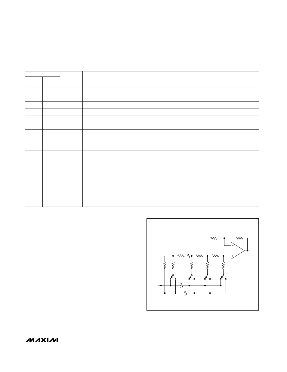
The DAC ladder outputs are buffered with op amps that
operate with a gain of two. The inverting node of the
amplifier is connected to the respective reference
input, resulting in bipolar output voltages from -REF_ to
4095/4096 REF_. Figure 1 shows the simplified DAC
circuit.
MAX547
Octal, 13-Bit Voltage-Output
DAC with Parallel Interface
_______________________________________________________________________________________
7
_________________________________________________Pin Description (continued)
FLAT
PACK
PLCC
NAME
FUNCTION
36
REFGH
Reference Voltage Input for DAC G and DAC H. Bypass to AGNDGH with a 0.1µF to 1µF capacitor.
30
16
A2
Address Bit 2
38
VOUTH
DAC H Output Voltage
33
–
L
—
D
—
G
—
H
–
Load Input (active low). Driving this asynchronous input low transfers the contents of input latches
G and H to the respective DAC latches.
32
35
AGNDGH
Analog Ground for DAC G and DAC H
34
GND
Digital Ground
PIN
10
27
29
28
41
VOUTE
DAC E Output Voltage
35
39
VOUTG
DAC G Output Voltage
33
40
VOUTF
DAC F Output Voltage
34
44
AGNDEF
38
Figure 1. DAC Simplified Circuit Diagram
2R
2R
R
D0
D10
D11
D12
R
R
R
R
OUT
REF–
AGND–
2R
2R
2R
V
DAC
43
REFEF
Reference Voltage Input for DAC E and DAC F. Bypass to AGNDEF with a 0.1µF to 1µF capaci-
37
32
–
L
—
D
—
E
—
F
–
Load Input (active low). Driving this asynchronous input low transfers the contents of input latches
E and F to the respective DAC latches.
26
17
A1
Address Bit 1
11
18
A0
Address Bit 0
19–31
D12–D0
Data Bits 12–0
13–25
12