Rainbow Electronics MAX547 User Manual
Page 11
load regulation is specified to 20ppm/mA max over
temperature, resulting in a maximum error of 36ppm
(90µV). This corresponds to a maximum error caused
by reference load regulation of only 0.147LSB
[0.147LSB = 90µV/(5V/8192)LSB] over temperature.
If you want a ±4.096V full-scale output swing (1LSB =
1mV), you can use the calibrated, low-drift, low-dropout
MAX676. Operating from a 5V supply, it is fully speci-
fied to drive two REF_ inputs with less than 60.4µV error
(0.0604LSB) over temperature, caused by the maxi-
mum load step.
Reference Buffering
Another way to obtain high accuracy is to buffer a refer-
ence with an op amp. When driving all reference inputs
simultaneously, keep the closed-loop output imped-
ance of the op amp below 0.03
Ω
to ensure an error of
less than 0.1LSB. The op amp must also drive the
capacitive load (typically 500pF to 1200pF).
Each reference input can also be buffered separately
by using the circuit in Figure 6. A reference load step
caused by a digital transition only affects the DAC pair
where the code transition occurs. It also allows the use
of references with little drive capability. Keep the
closed-loop output impedance of each op amp below
0.12
Ω
, to ensure an error of less than 0.1LSB. Figure 6
shows the op amp’s inverting input directly connected
to the MAX547’s reference terminal. This eliminates the
influence of board lead resistance by sensing the volt-
age with a low-current path sense line directly at the
reference input.
Adding feedback resistors to individual reference
buffer amplifiers enables different reference voltages to
be generated from a single reference.
MAX547
Octal, 13-Bit Voltage-Output
DAC with Parallel Interface
______________________________________________________________________________________
11
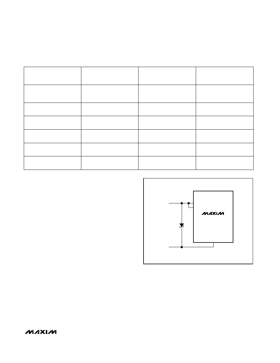
Figure 5. Optional Schottky Diode between V
SS
and GND
GND
V
SS
SYSTEM GND
1N5817
MAX547
V
SS
BIPOLAR OPERATION
(AGND_ = 0V)
CUSTOM OPERATION
POSITIVE UNIPOLAR
OPERATION
(AGND_ = REF_/2)
PARAMETER
AGND_ (=0V)
AGND–
Bipolar Zero Level, or
Unipolar Mid-scale,
(Code = 1000000000000)
REF–
REF– - AGND–
REF–/2
Differential Reference Voltage
(V
DR
)
REF_
AGND–
(
= ———
)
2
-REF–
AGND– - V
DR
0V
Negative Full-scale Output
(Code = All 0s)
4095
(
———
) (
REF_
)
4096
4095
AGND _ +
(
———
) (
V
DR
)
4096
8191
(
———
) (
REF_
)
8192
Positive Full-Scale Output
(Code = All 1s)
REF_
———
4096
V
DR
———
4096
REF_
(
———
)
8192
LSB Weight
D
(
——— - 1
) (
REF_
)
4096
D
AGND _ +
(
—--—- - 1
) (
V
DR
)
4096
D
(
———
) (
REF_
)
8192
VOUT
–
as a Function of
Digital Code (D, 0 to 8191)
Table 5. Reference, AGND– and Output Relationships