Rainbow Electronics MAX547 User Manual
Page 2
MAX547
Octal, 13-Bit Voltage-Output
DAC with Parallel Interface
2
_______________________________________________________________________________________
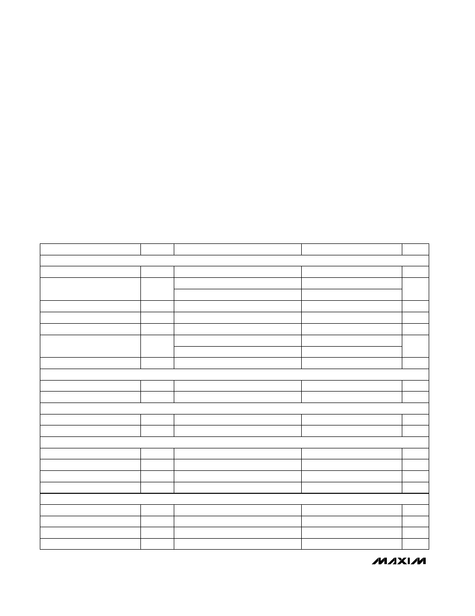
ABSOLUTE MAXIMUM RATINGS
ELECTRICAL CHARACTERISTICS
(V
DD
= +5V, V
SS
= -5V, REF_ = 4.096V, AGND_ = GND = 0V, R
L
= 10k
Ω
, C
L
= 50pF, T
A
= T
MIN
to T
MAX
, unless otherwise noted.
Typical values are at T
A
= +25°C.)
Stresses beyond those listed under “Absolute Maximum Ratings” may cause permanent damage to the device. These are stress rat-
ings only, and functional operation of the device at these or any other conditions beyond those indicated in the operational sections of
the specifications is not implied. Exposure to absolute maximum rating conditions for extended periods may affect device reliability.
V
DD
to GND ..............................................................-0.3V to +6V
V
SS
to GND ...............................................................-6V to +0.3V
Digital Input Voltage to GND ......................-0.3V to (V
DD
+ 0.3V)
REF_ ..........................................(AGND_ - 0.3V) to (V
DD
+ 0.3V)
AGND_ .............................................(V
SS
- 0.3V) to (V
DD
+ 0.3V)
VOUT_ ........................................................................V
DD
to V
SS
Maximum Current into REF_ Pin .......................................±10mA
Maximum Current into Any Other Signal Pin ....................±50mA
Continuous Power Dissipation (T
A
= +70°C)
PLCC (derate 13.33mW/°C above +70°C) ...................1067mW
Plastic FP (derate 11.11mW/°C above +70°C )..............889mW
Operating Temperature Ranges
MAX547–C–H.........................................................0°C to +70°C
MAX547–E–H......................................................-40°C to +85°C
Storage Temperature Range .............................-65°C to +150°C
Lead Temperature (soldering, 10sec) .............................+300°C
CONDITIONS
nV-s
5
Digital Crosstalk
nV-s
5
Digital Feedthrough
µs
5
Output Settling Time
V/µs
3
Voltage-Output Slew Rate
k
Ω
5
RREF
Reference Input Resistance
V
AGND
–
V
DD
REF
Reference Input Range
%/%
±0.0025
PSRR
Power-Supply Rejection Ratio
±0.0025
Bits
13
N
Resolution
LSB
Bipolar Zero-Code Error
±5
±20
±0.5
±2
LSB
±0.5
±4
INL
Relative Accuracy
LSB
±1
DNL
Differential Nonlinearity
UNITS
MIN
TYP
MAX
SYMBOL
PARAMETER
To ±
1
⁄
2
LSB of full scale (Note 4)
Each REF– pin (Note 3)
(Notes 2, 3)
MAX547A
MAX547B
∆
Gain/
∆
V
SS
(Note 1)
Guaranteed monotonic
∆
Gain/
∆
V
DD
(Note 1)
LSB
0.3
Load Regulation
R
L
=
∞
to 10k
Ω
LSB
Gain Error
±1
±8
STATIC PERFORMANCE—ANALOG SECTION
V
V
SS
+ 0.5
Minimum Output Voltage
V
V
DD
- 0.5
Maximum Output Voltage
pF
10
CIN
Input Capacitance
µA
1.0
IIN
Input Current
V
0.8
VIL
Input Voltage Low
V
2.4
VIH
Input Voltage High
(Note 5)
V
IN
= 0V or V
DD
ANALOG OUTPUT
REFERENCE INPUT
(Note 2)
DYNAMIC PERFORMANCE—ANALOG SECTION
DIGITAL INPUTS
(V
DD
= 5V ±5%)