Epson SED 1520 Series User Manual
Page 30
SED1520 Series
EPSON
2–21
SED1520
Series
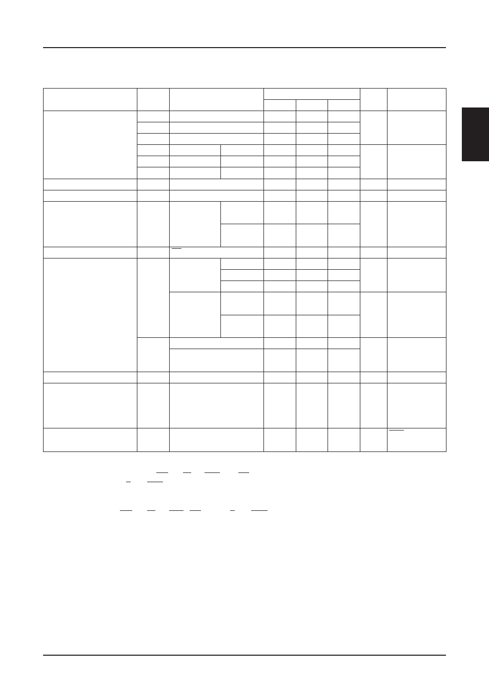
DC Characteristics (Cont’d)
Ta = –20 to 75 deg. C, V
DD
= 0 V unless stated otherwise
Rating
Parameter
Symbol
Condition
Unit
Applicable Pin
Min.
Typ.
Max.
V
OLT
I
OL
= 3.0 mA
—
—
V
SS
+0.4
OSC2
V
OLC1
I
OL
= 2.0 mA
—
—
V
SS
+0.4
V
See note 4 & 5.
V
OLC2
I
OL
= 120
µ
A
—
—
0.8
×
V
SS
Low-level output voltage
V
OLT
V
SS
= –3 V
I
OL
= 2 mA
0.8
×
V
SS
See note 4 & 5.
V
OLC1
V
SS
= –3 V
I
OL
= 2 mA
0.8
×
V
SS
V
OSC2
V
OLC2
V
SS
= –3 V
I
OL
= 50
µ
A
0.8
×
V
SS
Input leakage current
I
LI
–1.0
—
1.0
µ
A
See note 6.
Output leakage current
I
LO
–3.0
—
3.0
µ
A
See note 7.
V
5
= –5.0 V
—
5.0
7.5
SEG0 to 79,
LCD driver ON resistance
R
ON
Ta = 25 deg. C
k
Ω
COM0 to 15,
V
5
= –3.5 V
—
10.0
50.0
See note 11
Static current dissipation
I
DDQ
CS
= CL = V
DD
—
0.05
1.0
µ
A
V
DD
f
CL
= 2 kHz
—
2.0
5.0
V
DD
During display
R
f
= 1 M
Ω
—
9.5
15.0
µ
A
See note 12,
V
5
= –5.0 V
f
CL
= 18 kHz
—
5.0
10.0
13 & 14.
I
DD
(1)
During display f
CL
= 2 kHz
1.5
4.5
V
DD
Dynamic current dissipation
V
5
= –5 V
µ
A
See note 12 & 13.
V
SS
= –3 V
Rf = 1 M
Ω
6.0
12.0
During access t
cyc
= 200 kHz
—
300
500
I
DD
(2)
V
SS
= –3V,
µ
A
See note 8.
150
300
During access t
cyc
= 200 kHz
Input pin capacitance
C
IN
Ta = 25 deg. C, f = 1 MHz
—
5.0
8.0
pF
All input pins
R
f
= 1.0 M
Ω
±
2%,
15
18
21
V
SS
= –5.0 V
Oscillation frequency
f
OSC
kHz
See note 9.
R
f
= 1.0 M
Ω
±
2%,
11
16
21
V
SS
= –3.0 V
RES
Reset time
t
R
1.0
—
µ
S
See note 15.
Notes: 1. Operation over the specified voltage range is guaranteed, except where the supply voltage changes
suddenly during CPU access.
2. A0, D0 to D7, E (or RD), R/W (or WR) and CS
3. CL, FR, M/S and RES
4. D0 to D7
5. FR
6. A0, E (or RD), R/W (or WR), CS, CL, M/S and RES
7. When D0 to D7 and FR are high impedance.
8. During continual write acess at a frequency of t
cyc
. Current consumption during access is effectively
proportional to the access frequency.
9. See figure below for details
10. See figure below for details
11. For a voltage differential of 0.1 V between input (V
1
, …, V
4
) and output (COM, SEG) pins. All voltages
within specified operating voltage range.
12. SED1520
*
A
*
and SED1521
*
A
*
and SED1522
*
A
*
only. Does not include transient currents due to
stray and panel capacitances.
13. SED1520
*
0
*
and SED1522
*
0
*
only. Does not include transient currents due to stray and panel
capacitances.
14. SED1521
*
0
*
only. Does not include transient currents due to stray and panel capacitances.
15. t
R
(Reset time) represents the time from the RES signal edge to the completion of reset of the internal
circuit. Therefore, the SED1520 series enters the normal operation status after this t
R
.