Sed1520 series epson, Display start line and line count registers, Column address counter – Epson SED 1520 Series User Manual
Page 18: Page register, Display data ram
SED1520 Series
EPSON
2–9
SED1520
Series
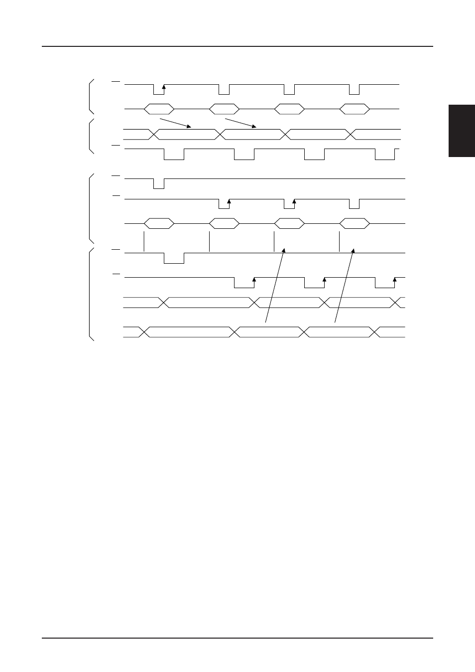
Figure 1 Bus Buffer Delay
Busy flag
When the Busy flag is logical 1, the SED1520 series is
executing its internal operations. Any command other
than Status Read is rejected during this time. The Busy
flag is output at pin D7 by the Status Read command. If
an appropriate cycle time (tcyc) is given, this flag needs
not be checked at the beginning of each command and,
therefore, the MPU processing capacity can greatly be
enhanced.
Display Start Line and Line Count
Registers
The contents of this register form a pointer to a line of
data in display data RAM corresponding to the first line
of the display (COM0), and are set by the Display Start
Line command. See section 3.
The contents of the display start line register are copied
into the line count register at the start of every frame, that
is on each edge of FR. The line count register is
incremented by the CL clock once for every display line,
thus generating a pointer to the current line of data, in
display data RAM, being transferred to the segment
driver circuits.
Column Address Counter
The column address counter is a 7-bit presettable counter
that supplies the column address for MPU access to the
display data RAM. See Figure 2. The counter is
incremented by one every time the driver receives a Read
or Write Display Data command. Addresses above 50H
are invalid, and the counter will not increment past this
value. The contents of the column address counter are set
with the Set Column Address command.
Page Register
The page resiter is a 2-bit register that supplies the page
address for MPU access to the display data RAM. See
Figure 2. The contents of the page register are set by the
Set Page Register command.
Display Data RAM
The display data RAM stores the LCD display data, on a
1-bit per pixel basis. The relation-ship between display
data, display address and the display is shown in Figure
2.
N
N + 1
N + 1
N + 2
N + 2
N + 3
N + 3
N
N + 1
N + 2
N
n
n + 1
n + 2
N
DATA
Bus
hold
WR
MPU
Internal
timing
MPU
Internal
timing
READ
WRITE
WR
WR
DATA
WR
RD
Column
address
Bus
hold
N
n
n + 1
N
Address set
at N
Dummy read
Data read
at N
Data read
at N + 1
RD