Sed1520 series epson, 3) lcd drive circuit signals – Epson SED 1520 Series User Manual
Page 16
SED1520 Series
EPSON
2–7
SED1520
Series
(3) LCD Drive Circuit Signals
Name
Description
CL
Input. Effective for an external clock operation model only.
This is a display data latch signal to count up the line counter and common counter
at each signal falling and rising edges. If the system has a built-in oscillator, this is
used as an output pin of the oscillator amp and an Rf oscillator resistor is con-
nected to it.
FR
Input/output.
This is an I/P pin of LCD AC signals, and connected to the M terminal of common
driver.
I/O selection
• Common oscillator built-in model:
Output if M/S is 1;
Input if M/S is 0.
• Dedicate segment model:
Input
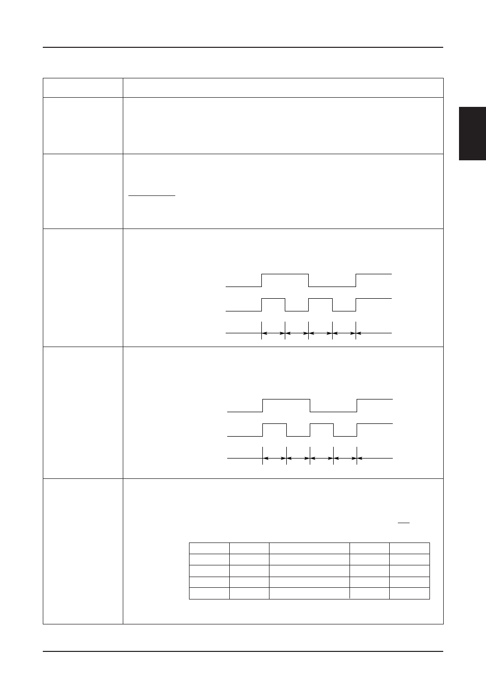
SEGn
Output.
The output pin for LCD column (segment) driving. A single level of V
DD
, V
2
, V
3
and
V
5
is selected by the combination of display RAM contents and RF signal.
1
0
1
0
1
0
V
V2
V5
V3
DD
FR signal
Data
Output level
COMn
Output.
The output pin for LCD common (low) driving. A single level of V
DD
, V
1
, V
4
and V
5
is selected by the combination of common counter output and RF signal. The
slave LSI has the reverse common output scan sequence than the master LSI.
1
0
1
0
1
0
V
V1
V5
V4
DD
FR signal
Counter output
Output level
M/S
Input.
The master or slave LSI operation select pin for the SED1520 or SED1522.
Connected to V
DD
(to select the master LSI operation mode) or V
SS
(to select the
slave LSI operation mode).
When this M/S pin is set, the functions of FR, COM0 to COM15, OSC1 (CS), and
OSC2 (CL) pins are changed.
* The slave driver has the reverse common output scan sequence than the master
driver.
M/S
FR
COM output
OSC1
OSC2
SED1520F
0A
V
DD
Output
COM0 to COM15
Input
Output
V
SS
Input
COM31 to COM16
NC
Input
SED1522F
0A
V
DD
Output
COM0 to COM7
Input
Output
V
SS
Input
COM15 to COM8
NC
Input