Avago Technologies ACPL-P347-000E User Manual
Page 2
2
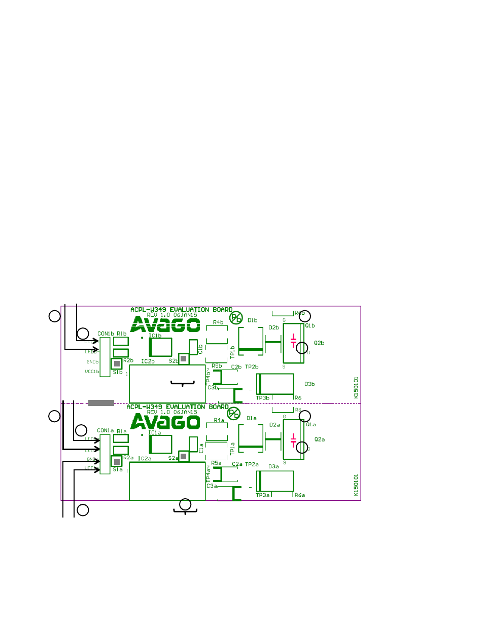
Once inspection is performed, the evaluation board can be used to test either one of the top and bottom half bridge
inverter arms in simulation mode without the need for a IGBT or SiC/GaN MOSFET. To perform testing simply follow the
five steps as outlined below (See Figure 2).
Testing both Arms of The Half Bridge Inverter Driver (without IGBT or SiC/GaN MOSFET)
1. Solder a 10nF capacitor across Gate and Emitter/Collector terminals of Q1 or Q2 (to simulate actual gate capacitance
of IGBT or SiC/GaN MOSFET)
2. Connect a +5V DC supply (DC supply 1) across +5V and GND terminals of CON1
3. Connect another DC supply (DC supply 2 with voltage range from 15V~30V) across Vcc2 (pin-7 of IC2) and Vee (pin-5
of IC2) terminals of IC2a respectively. This can be non-isolated for testing purposes
4. Connect drive signals;
a) A 10kHz 5V DC pulse (at slightly <50% duty) from a dual output signal generator across IN1+ & IN1- pins of CON1a
to simulate microcontroller output to drive lower arm of the half bridge Inverter
b) Another 10kHz 5V DC pulse (at 180
° out of phase to 4a) from the dual output signal generator across IN2+ & IN2-
pins of CON1b to simulate microcontroller output to drive upper arm of the half bridge Inverter
5. Use a multi-channel digital oscilloscope to capture the waveforms at the following points;
a. LED signal at IN1+ pin with reference to GND
b. LED signal at IN2+ pin with reference to GND
Note: Vcc2b supply of voltage close to Vcc2a should then be successfully generated through the built-in bootstrap components D3b and R6.
c. Vga representing the output voltage of ACPL-P349/W349 (IC1a) at Gate pin of Q1a (or Q2a) with reference to Vea
d. Vgb (through an isolated probe) representing the output voltage of ACPL-P349/W349 (IC1b) at Gate pin of Q1b (or
Q2b) with reference to Veb
Figure 2. Simulation Test Setup of Evaluation Board
10nF
In1+
In1
-
Signal Input
+5V
Gnd
DC Supply1
15~30V
+
-
10nF
Vcc2b
+
-
In2+
In2
-
Signal Input
5a
5c
5d
Vea
Veb
DC Supply2
1
2
4a
3
1
4b
5b