Using the boards as a design reference, In closing, Usb host interface board schematic – Linx Technologies MDEV-xxx-ES User Manual
Page 9: Rs232 host interface board schematic, Rf section schematic, Figure 10: usb host interface board schematic
–
–
–
–
12
13
Using the Boards as a Design Reference
The master development boards included in this kit are very simple, yet
they illustrate some important techniques that should be incorporated
into the board layout. The module’s mounting pads extend slightly past
the edge of the part. This eases hand assembly and allows for better
heat conduction under the part if rework is necessary. A full ground plane
fill is placed on the bottom of the board. This ground plane serves three
important purposes:
First, since a quarter-wave antenna is employed, the ground plane is
critical to serve as a counterpoise (please see Application Note AN-00500
“Antennas: Design, Application, and Performance” for details on how a
ground plane affects antenna function).
Second, a ground plane will suppress the transfer of noise between stages
of a product, as well as unintentional radiation of noise into free space.
Third, a ground plane allows for the implementation of a microstrip feed
between the module and the antenna. The term microstrip refers to a PCB
trace running over a ground plane that is designed to serve as a 50-ohm
transmission line. See the ES Series data guide or the calculator available
on our website for details on microstrip calculations.
In Closing
Here at Linx, “Wireless Made Simple” is more than just our motto, it is our
commitment. A commitment to the highest caliber of product, service,
and support. That is why, should you have questions or encounter any
difficulties using the evaluation kit, you’ll be glad to know many resources
are available to assist you. First, check carefully for the obvious, then
visit our website at www.linxtechnologies.com or call +1 541 471 6256
between 8AM and 4PM Pacific Time to speak with an application engineer.
RX DATA
AUDIO
RSSI
RX PDN
RX RS232 SQ
RX DEC
AUDIO REF
1
2
3
4
5
6
7
8
9
TS2
CON9
GND
TX = NS
RX RS232 SQ
R26
10K
R25
10K
R23
10K
R24
2M
AUDIO REF
AUDIO
VCC
VCC
R19
39K
R20
2M
R18
10K
R21
39K
C2
0.01uF
VCC
GND
GND
GND
GND
RSSI
R22
390K
R17
5K
OUTA
1
INA-
2
INA+
3
GND
4
INB+
5
INB-
6
OUTB
7
VCC
8
U6
LMV393
R28
0
R27
0
TX = NS
VCC
VCC
11
12
13
14
15
16
17
18
19
20
GND
R7
100k
GND
R8
100k
GND
R9
100k
GND
R10
100k
GND
GND
TX ENC
1
2
3
4
5
6
7
8
9
10
GND
R2
200
R3
100k
R4
100k
GND
R6
100k
GND
R5
100k
GND
GND
VCC
GND
VCC
SW2
SEL_BAUD0
SW3
SEL_BAUD1
GND
LATCH
D2
MODE_IND
PDN ENC
GN
D
BZ
1
BUZZE
R
B`
4
C
5
C`
6
GN
D
7
B
3
A`
2
A
1
E
11
F`
12
F
13
VC
C
14
E`
10
D
9
D`
8
U5
CD4069UB HEX INVERTE
R
C3
0.01uF
R15
100k
R16
10k
TX = NS
S0
BUZZE
R
VC
C
GN
D
R0
100k
SEN
D
D0
0805_DIOD
E
RX = NS
RE
1
RELAY-SPD
T
1
2
J2
RELAY OU
T
GN
D
GN
D
C4
10uF
TX = NS
S1
RELAY
VC
C
GN
D
R1
100k
SEND
D1
0805_DIODE
RX = NS
S3
CREATE/LEARN
RX DEC
VCC
GND
R12
100k
SEND
R13
100k
GND
RX = NS
D6
D7
SEL_BAUD0
SEL_BAUD1
GND
GND
D_LATCH/E_GND
D_RX_CNTL/E_TX_CNTL
D_TX_ID/E_DATA_OUT
MODE_IND
D_LEARN/E_CREATE
D_DATA_IN/E_SEND
D0
D1
VCC
VCC
D2
D3
D4
D5
U4
LICAL-ENC/DEC-MS
TX = ENC
RX = DEC
VCC
GND
GND
GND
GND
TX RS232
RX RS232 SQ
GND
1
NC
2
NC
3
NC
4
VCC
5
NC
6
NC
7
GND
8
GND
9
DTR/PDN
10
RTS/TRSEL
11
TX DATA
12
RX DATA
13
NC
14
NC
15
GND
16
J3
HOST MODULE
PDN RS232
TX DATA
TX PDN
TX RS232
/CLK
TX ENC
/CLK SEL
GND
LO V DET
RX = NS
PDN RS232
PDN ENC
1
2
3
4
5
6
7
8
9
10
11
TS1
CON11
RX PDN
RSSI
RX DATA
AUDIO
AUDIO REF
VCC
GND
GND
ANT
1
GND
2
NC
3
GND
4
VCC
5
NC
6
NC
7
NC
8
NC
9
A REF
10
AUDIO
11
DATA
12
RSSI
13
PDN
14
NC
15
NC
16
U3
RXM-XXX-ES
TX = NS
TX PDN
TX DATA
LO V DET
/CLK SEL
/CLK
GND
GND
R14
220 ohm
VCC
PDN
1
LADJ
2
VCC
3
GND
4
DATA
5
/CLK
6
/CLK SEL
7
LO_V_D
8
GND
9
ANT
10
U2
TXM-XXX-ES
R29
22K
GND
RX = NS
RF
GND
GND
1
2-
5
ANT1
CONREVSMA001
RF SECTION
ENCODER/DECODER SECTION
Host Interface Header
Proto Signal Header
B1
9V BATTERY
GND
SW1
POWER SWITCH
GND
+ C1
220uF
GND
VCC
D11
DIODE400
J1
PWRJACK
GND
Vin
1
GND
2
Vout
3
U1
LM7805 5V REGULATOR
POWER SUPPLY SECTION
HEADER SECTION
SQUELCH CIRCUIT
RS232 HOST INTERFACE BOARD
USB HOST INTERFACE BOARD
U1
C3
C4
C5
C1
J2
C2
3.3uF
3.3uF
3.3uF
MAX232
3.3uF
RS-232
4.7uF
C1+
V+
C1-
C2+
C2-
V-
T2OUT
R2IN
R2OUT
T2IN
T1IN
R1OUT
R1IN
T1OUT
GND
VCC
VCC
GND
GND
VCC
GND
GND
TX RS232
RX RS232
PDN
TR SEL
1
2
3
4
5
6
7
8
9
10
11
12
13
14
15
16
1
6
2
7
3
8
4
9
5
J1
HIB-DIPMODULE
GND
NC
NC
NC
VCC
NC
NC
GND
GND
DTR/PDN
RTS/TRSEL
TX DATA
RX DATA
NC
NC
GND
GND
GND
GND
GND
VCC
TX RS232
RX RS232
PDN
TR SEL
1
2
3
4
5
6
7
8
9
10
11
12
13
14
15
16
+
+
+
+
+
J1
HIB-DIPMODULE
GND
GND
GND
GND
GND
NC
NC
NC
VCC
NC
NC
GND
GND
DTR/PDN
RTS/TRSEL
TX DATA
RX DATA
NC
NC
GND
TX DATA
RX DATA
PDN
TRSEL
1
2
3
4
5
6
7
8
9
10
11
12
13
14
15
16
USBDP
USBDM
GND
DSR
DATA_IN
DATA_OUT
RTS
CTS
DTR
TX_IND
VCC
SUSP_IND
RX_IND
485_TX
RI
DCD
1
2
3
4
5
6
7
8
9
10
11
12
13
14
15
16
USB-B
GND
5V
DAT -
DAT+
GND
GSHD
GSHD
GND
GND
1
2
3
4
5
6
GND
SDM-USB-QS-S
J2
TX DATA
RX DATA
TRSEL
PDN
U1
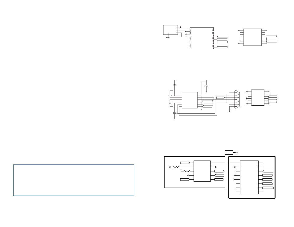
USB Host Interface Board Schematic
Figure 10: USB Host Interface Board Schematic
RS232 Host Interface Board Schematic
RS232 HOST INTERFACE BOARD
USB HOST INTERFACE BOARD
U1
C3
C4
C5
C1
J2
C2
3.3uF
3.3uF
3.3uF
MAX232
3.3uF
RS-232
4.7uF
C1+
V+
C1-
C2+
C2-
V-
T2OUT
R2IN
R2OUT
T2IN
T1IN
R1OUT
R1IN
T1OUT
GND
VCC
VCC
GND
GND
VCC
GND
GND
TX RS232
RX RS232
PDN
TR SEL
1
2
3
4
5
6
7
8
9
10
11
12
13
14
15
16
1
6
2
7
3
8
4
9
5
J1
HIB-DIPMODULE
GND
NC
NC
NC
VCC
NC
NC
GND
GND
DTR/PDN
RTS/TRSEL
TX DATA
RX DATA
NC
NC
GND
GND
GND
GND
GND
VCC
TX RS232
RX RS232
PDN
TR SEL
1
2
3
4
5
6
7
8
9
10
11
12
13
14
15
16
+
+
+
+
+
J1
HIB-DIPMODULE
GND
GND
GND
GND
GND
NC
NC
NC
VCC
NC
NC
GND
GND
DTR/PDN
RTS/TRSEL
TX DATA
RX DATA
NC
NC
GND
TX DATA
RX DATA
PDN
TRSEL
1
2
3
4
5
6
7
8
9
10
11
12
13
14
15
16
USBDP
USBDM
GND
DSR
DATA_IN
DATA_OUT
RTS
CTS
DTR
TX_IND
VCC
SUSP_IND
RX_IND
485_TX
RI
DCD
1
2
3
4
5
6
7
8
9
10
11
12
13
14
15
16
USB-B
GND
5V
DAT -
DAT+
GND
GSHD
GSHD
GND
GND
1
2
3
4
5
6
GND
SDM-USB-QS-S
J2
TX DATA
RX DATA
TRSEL
PDN
U1
Figure 11: RS232 Host Interface Board Schematic
RF Section Schematic
Figure 12: RF Section Schematic
Legal Notice:
All Linx kits and modules are designed in keeping with
high engineering standards; however, it is the responsibility of the user to
ensure that the products are operated in a legal and appropriate manner.
The purchaser understands that legal operation may require additional
permits, approvals, or certifications prior to use, depending on the
country of operation.