The prototyping area, Using the simplex encoder / decoder section, Using the data squelch circuit – Linx Technologies MDEV-xxx-ES User Manual
Page 6
–
–
–
–
6
7
The Prototyping Area
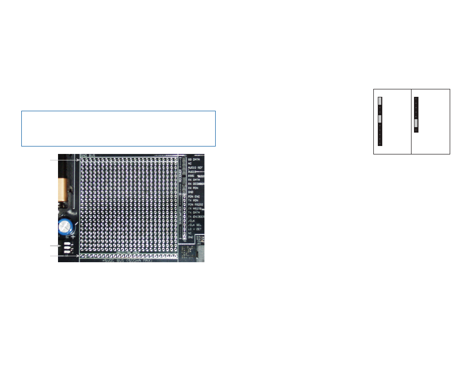
In addition to their evaluation functions, the boards may also be used
for actual product development. They feature a prototyping area for the
addition of application-specific circuitry. The prototyping area is the same
on both boards and contains a large area of plated through-holes so that
external circuitry can be placed on the board. The holes are set at 0.1" on
center with a 0.04" diameter, making it easy to add most industry-standard
SIP and DIP packages to the board. This circuitry can be interfaced with
the ES transmitter or receiver through the breakout header to the right. At
the bottom of this area is a row connected to the 5V power supply and at
the top is a row connected to ground.
Note:
The on-board 5-volt regulator has approximately 500mA of
headroom available for additional circuitry. If added circuitry requires a
higher current, the user must add an additional regulator to the prototype
area or power the board from an external supply.
Ground Bus
Regulator
+5 Volt Bus
Figure 5: The Development Board Prototyping Area
Using the Simplex Encoder / Decoder Section
The transmitter board features an MS Series remote control encoder with
two push buttons and the receiver board features a decoder with a relay
output and a buzzer. When a button is pressed on the transmitter board,
the status of both buttons is captured and encoded into a data stream
for transmission. The data recovered by the receiver is decoded and the
decoder’s outputs are set to replicate the states of the encoder, driving
either the buzzer or the relay.
To activate this area of the board, the
module DATA line must be routed to
the encoder / decoder. Configure the
transmitter board for encoding and
transmission by placing a jumper across TX
DATA and ENCODER and across TX PDN
and PDN ENC on header TS1. Configure
the receiver board for reception and
decoding by placing a jumper across RX
DATA and DECODER on header TS2.
Once the boards have been configured, place the receiver board on a flat
surface and turn it on. Turn on the transmitter board and press button S0.
You should hear the buzzer on the receiver board sound. Walk away from
the receiver to ascertain the useable range of the link in the environment.
Button S1 activates the relay on the receiver board. The relay’s SPST
contacts can be connected at J2. Any device up to 5A at 30VDC / 120VAC
may be switched through the relay. An external siren or light can be
connected to aid range testing if the on-board buzzer is not loud enough.
Using the Data Squelch Circuit
A data squelch circuit is provided on the receiver development board.
This circuit is used to add both hysteresis and squelching capabilities as
detailed in the ES Series Receiver Data Guide. Since the ES Series receiver
output is not internally squelched, its output continually switches when no
transmission is present. This can cause interrupts and buffer overflows in
external circuitry. A squelch circuit helps eliminate this noise by providing
a qualification threshold for incoming data based on signal strength. This
circuit is not a substitute for robust protocol since squelch can be broken
by unintended interference.
TS1
TX
RX
TS2
SQ. DATA
NC
AUDIO REF
AUDIO
RSSI
RX DATA
RX DECODER
RX PDN
PDN ENC
TX PDN
PDN RS232
TX RS232
TX DATA
TX ENCODER
/CLK
/CLK SEL
LO V DET
NC
GND
TS1
TX
RX
TS2
SQ. DATA
NC
AUDIO REF
AUDIO
RSSI
RX DATA
RX DECODER
RX PDN
PDN ENC
TX PDN
PDN RS232
TX RS232
TX DATA
TX ENCODER
/CLK
/CLK SEL
LO V DET
NC
GND
Figure 6: Jumper Configuration