Chapter 3, Board layout – Lanner LEC-2136 User Manual
Page 14
14
Board Layout
Chapter 3
Embedded and Industrial Computing
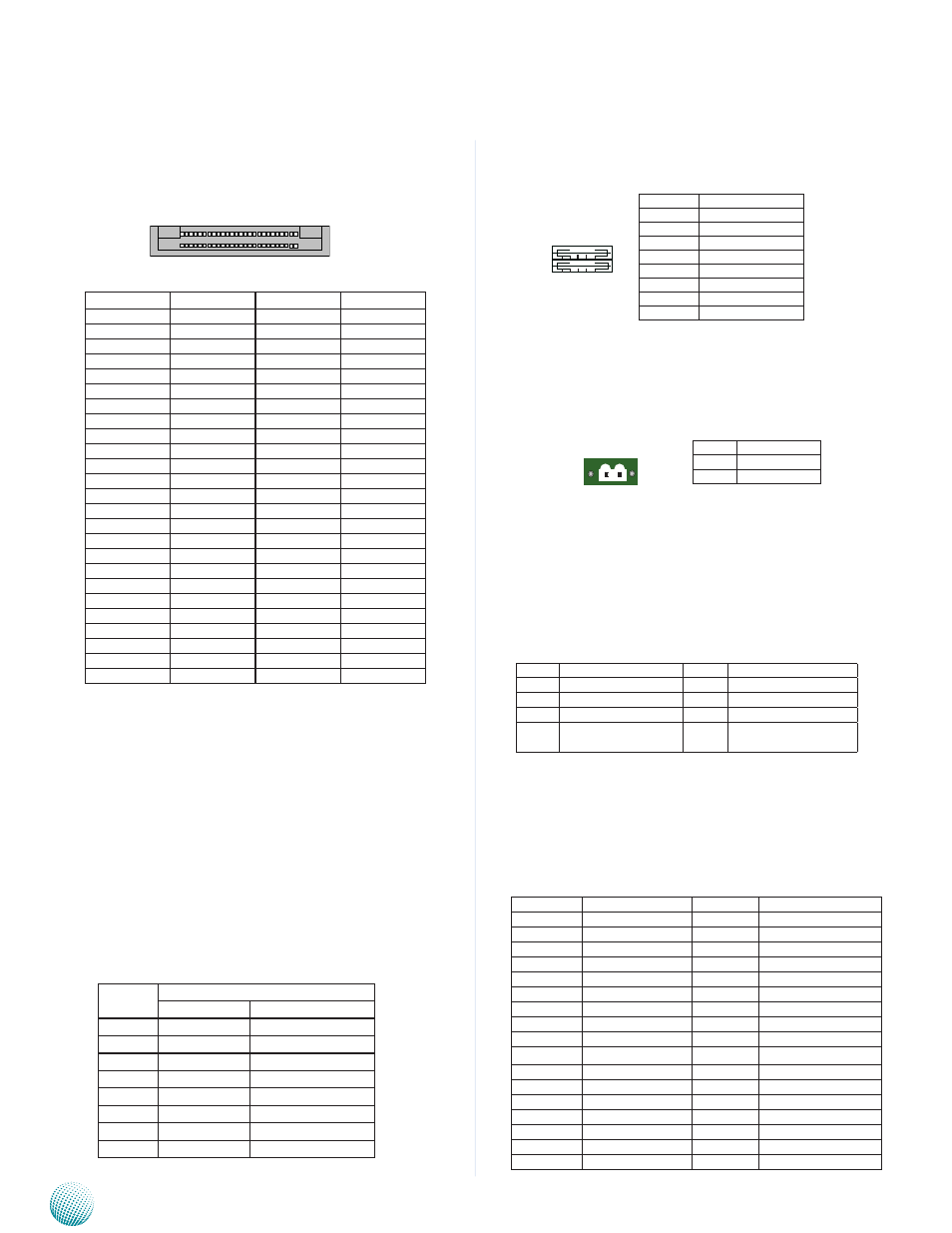
CompactFlash Connector (CN4): It is for connecting a
Compact Flash card to be served as your system’s storage.
Pin No.
Function
Pin No.
Function
1
GND
26
CF_CD1#
2
CF_DD3
27
CF_DD11
3
CF_DD4
28
CF_DD12
4
CF_DD5
29
CF_DD13
5
CF_DD6
30
CF_DD14
6
CF_DD7
31
CF_DD15
7
CF_DCS0#
32
CF_DCS1#
8
A10(GND)
33
VS1#
9
OE#(GND)
34
CF_DIOR#
10
A9(GND)
35
CF_DIOW#
11
A8(GND)
36
WE#(VCC3)
12
A7(GND)
37
CF_IRQ#
13
VCC
38
VCC
14
A6(GND)
39
CSEL#(GND)
15
A5(GND)
40
VS2#
16
A4(GND)
41
CF_RESET#
17
A3(GND)
42
CF_IORDY
18
CF_A2
43
CF_DMARQ
19
CF_A1
44
CF_DDACK#
20
CF_A0
45
CF_ACT#
21
CF_DD0
46
CF_DIAG
22
CF_DD1
47
CF_DD8
23
CF_DD2
48
CF_DD9
24
WP(NC)
49
CF_DD10
25
CF_CD2#
50
GND
LAN1/LAN2/LAN3 Ports: The LAN ports are provided by
Intel 82574L(the management port on LAN 1) and 82583V
Ethernet Controllers. The following lists its main features:
PXE remote boot
•
TCP segmentation offload, TCP, UDP, IPv4 checksum
•
offload
The 82574L has more advanced features such as:
Interrupt moderation, VLAN support, jumbo frames,
•
RSS, MSI, MSI-X
IPMI pass-through via SMBus or NC-SI, WoL, PXE
•
remote boot, ISCSI boot, VLAN filtering
Supports IEEE 802.1Q VLAN tagging
•
Pin No. Description
Fast Ethernet Gigabit Ethernet
1
TX+
BI_DA+
2
TX-
BI_DA-
3
RX+
BI_DB+
4
--
BI_DC+
5
--
BI_DC-
6
RX-
BI_DB-
7
--
BI_DD+
8
--
BI_DD-
25 1
50 26
Dual USB 2.0 Port Connector #1 and #2 (CN7):
Dual USB 2.0 Port Connector #3and #4 (CN10)
DC_IN Power Connector (CN9): This connector is
provided power in connector.
Front Panel Power Button (CN2): It provides redundant
LED signal and button function on the front panel.
Red: System standby
Green: System power-on
Mini PCI Express Connector (CN6): t is for connecting
WiFi module to serve Wireless LAN connections or con-
necting Wireless 3G module for mobile Internet connec-
tions. The socket supports only Universal Serial Bus (USB)
signal type PCIe card.
PIN
Pin Name
PIN
Pin Name
1
WAKE#
27
GND
2
VCC3
28
1.5V
3
RSV1
29
GND
4
GND
30
SMB_CLK
5
RSV2
31
NC(PETn)
6
1.5V
32
SMB_DATA
7
CLKREQ#
33
NC(PETp)
8
UIM_PWR
34
GND
9
GND
35
GND
10
UIM_DATA
36
USB_D-
11
NC(REFCLK-)
37
RSV5
12
UIM_CLK
38
USB_D+
13
NC(REFCLK+)
39
RSV6
14
UIM_RST
40
GND
15
GND
41
RSV7
16
UIM_VPP
42
LED_WWAN#
17
RSV3
43
RSV8
Pin No.
Pin Name
1
USB power
2
USB0_DAT-
3
USB0_DAT+
4
Signal Ground
5
USB power
6
USB1_DAT-
7
USB1_DAT+
8
Signal Ground
1 2 3 4
5 6 7 8
Pin No.
Pin Name
1
DC_GND
2
DC_IN
1 2
Pin No.
Pin Name
Pin No.
Pin Name
PAD1
Ground
PAD2
Ground
1
Ground
3
BUTTON-
2
Ground
4
BUTTON-
L1
PWR_LED+ /
STB_LED-
L2
PWR_LED- /
STB_LED+