Chapter 3, Board layout, Jumper settings – Lanner LEC-2136 User Manual
Page 13
13
Board Layout
Chapter 3
Embedded and Industrial Computing
RS-232 Serial Port NO. 2(J9): It is a RS-232 port via the
internal pin header.
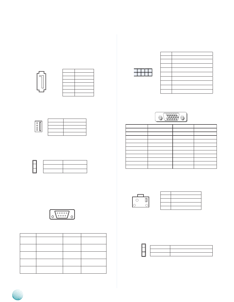
DB-15 VGA Connector (VGA1)
Pin No.
Description
Pin No.
Description
1
RED
6
CRT DET
2
GREEN
7
GND
3
BLUE
8
GND
4
N/A
9
VCC5
5
GND
10
GND
Pin No.
Description
11
N/A
12
DDC DATA
13
HSYNC
14
VSYNC
15
DDC CLK
Front Panel Reset Button (SW1)
Hardware or Software Reset Selection (JP2): The reset
function (SW1) can be selected to be as a software reset or
hardware reset. The software reset can set the designated
software to its default settings. The hardware reset will
trigger the reset signal and reboot the whole system.
Jumper Settings
Serial-ATA Connector (J6): It is for connecting a 2.5’’
harddisk to be served as your system’s storage. It can
support SATA II which features Data transfer rates up to
3.0 Gb/s (300 MB/s).
4-pin Serial-ATA Power Connector (J8): It is for
connecting the SATA power cord.
Clear CMOS jumper (JP1): It is for clearing the CMOS
memory.
RS-232 Serial Port NO. 1 (COM1): It is a RS-232 port
through the D-SUB9 connector.
Pin No.
Pin Name
Pin No.
Pin Name
1
Data Carrier Detect
(DCD)
6
Data Set Ready
(DSR)
2
Received Data
(RxD)
7
Request To Send
(RTS)
3
Transmitted Data
(TxD)
8
Clear To Send
(CTS)
4
Data Terminal
Ready (DTR)
9
RIA
5
Signal Ground
(GND)
LEB-2136
Pin No.
Function
1
VCC12 (12V)
2
Ground
3
Ground
4
VCC (5V)
Pin No.
Pin Name
1
Data Carrier Detect (DCD)
2
Received Data (RxD)
3
Transmitted Data (TxD)
4
Data Terminal Ready (DTR)
5
Signal Ground
6
Data Set Ready (DSR)
7
Request To Send (RTS)
8
Clear To Send (CTS)
9
Ring Indicator (RI)
1 2 3 4 5
6 7 8 9
Pin No.
Function
1
Ground
2
Ground
3
TX+
4
TX-
5
Ground
6
RX-
7
RX+
7
6
5
4
3
2
1
SATA1
4
3
2
1
Pin No.
Pin Name
1-2
Normal (Default)
2-3
Clear CMOS
1
2
3
1 3 5 7 9
2 4 6 8 1 0
1
3
2
4
Pin No.
Pin Name
1
reset signal
2
GND
3
NC
4
GND
Pin No.
Description
1-2 (Default)
Software Reset
2-3
Hardware Reset
3
2
1
5
10
15
1
6
11