Unit configuration, Configuration switchs1, Configuration – Verilink PRISM 4051 (34-00253.2) Product Manual User Manual
Page 12: Switch s1
6
C
HAPTER
2: I
NSTALLATION
Unit
Configuration
The PRISM 4051 can be hardware configured by switches or software configured
by using a terminal connection to the front panel supervisory access (SUPV) port.
The terminal interface provides more capabilities than the configuration switches.
If there is a power failure, the 4051 retains its configuration in non-volatile
memory. This feature allows the unit to automatically restore normal service
following a power loss. See section Utilities on page 37 for more information.
The 4051 stores its operating firmware in Flash memory. If a software upgrade is
ever needed, Verilink will provide the hex files, the download program, and the
downloading instructions.
Hardware switches on the circuit boards allow configuring most simple
applications. These switches are described in the following paragraphs. If an
ambiguous configuration is programmed, the unit overrides invalid configuration
items.
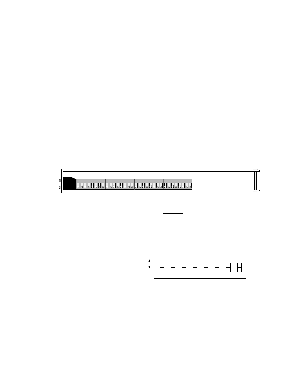
The unit is hardware configured using four DIP switches located on the upper side
between the circuit boards (see Figure 2-1). Switch positions are numbered as
follows: position 2 of Switch S3 is referred to as Switch S3-2, and so on.
Before installation, verify each configuration switch setting.
Factory default settings are shown underlined throughout this manual.
Configuration
Switch S1
Switch S1 (Figure 2-2) is
used to set the configuration
for boot mode; DDS mode;
timing source; RTS-to-CTS
delay; RTS, CTS, and DCD
handshake; local and remote
loopback enable; and DTE
alarm.
1 2 3 4 5 6 7 8
1 2 3 4 5 6 7 8
1 2 3 4 5 6 7 8 1 2 3 4 5 6 7 8
Switch 1
Switch 2
Switch 3
Switch 4
Figure 2-1 Top View of the PRISM 4051
✍
7
6
5
4
3
2
1
Do
wn
Up
8
Boot
DDS I
/
Ti
m
ing
LL and
RL
DTE
M
ode
Al
ar
m
Ena
b
le
R
T
S,
CTS,
and
DCD Ha
n
d
sh
a
k
e
Sou
rc
e
Ti
m
ing
Sou
rc
e
RT
S
-t
o
-C
T
S
De
la
y
Switch
S1
Figure 2-2 Switch S1
DDSI
I