5 on-board reset, 6 clock circuitry (optional) – Sundance SMT166 User Manual
Page 22
4.2.5
On-board reset
A push button is dedicated to reset the board, and clear and reload the FPGA
configuration. It is coupled with a reset chip in order to avoid multiple resets.
The reset signal only goes to the CPLD. The CPLD then propagates the reset signal to
the FPGAs and other peripherals such as the USB circuitry.
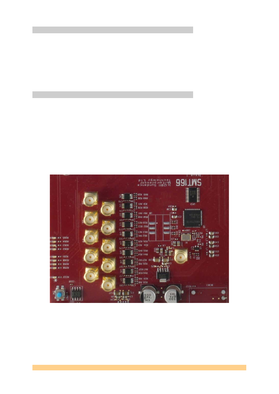
The button is located as shown below – bottom left.
4.2.6
Clock circuitry (optional)
The optional clock circuitry is built around a CDCE72010 from Texas Instrument. It
is a clock synchroniser, jitter cleaner and clock distributor.
When coupled with a VCXO, it can be locked to a reference signal and generate
synchronised in phase and frequency outputs, which can then be used on SLB
mezzanine modules present on the SMT166.
The clock chip requires programming through its serial interface port. Serial lines
are connected to the first FPGA.
The clock circuitry is physically isolated from the rest of the board in order to
reduce potential electrical disturbances.
Product Specification SMT166
Page 22 of 44
Last Edited: 17/06/2014 16:12:00