4 ddr3 memory – Sundance SMT166 User Manual
Page 21
4.2.4
DDR3 Memory
The SMT166 has got four independent DDR3 memory banks. Each Virtex6 FPGA is
responsible for providing access to two banks. Memory chips used are
manufactured by Micron and can be clocked at up to 666MHz (DDR3-1333). In a
more reasonable approach, a 400MHz memory clock will allow storing 3.2Gbytes/s
and per bank. For power consumption reasons, the clock frequency is brought
down.
-1 speed grade FPGA will only allow the DDR3 interfaces to work at 400MHz. Fitting
a -2 and -3 FPGA will give access to the full speed of 533MHz. The limitation here is
the FPGA.
Each memory bank is 32-bit wide and made out of 2 memory chips (MT41J64M16xx-
15E – 2Gbit part) and can store up to 256 Mbytes of data. Memory chips are
powered under 1.5 Volts (Vdd and Vddq) and can take up to 430mA each. The board
counts in total 16 chips, giving a total of nearly 7Amps.
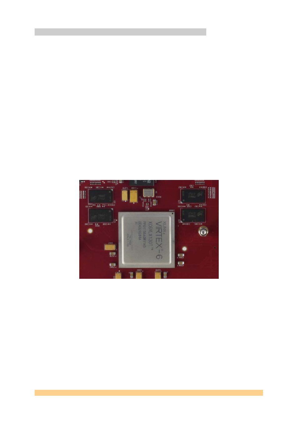
This image shows the Virtex-6 FPGA and its two associated DDR3 memory banks
(two devices per bank).
DDR3 memory also requires a reference voltage (half of the supply voltage,
Vrefdq=0.75 Volt). The current required for the reference level is negligible
compared to the supply voltage but must coming from a sink/source regulator.
14mA per chip gives a total of 224mA.
The FPGAs will use their internal reference voltage, derived from the FPGA bank
power supply (Vcco). Active terminations are also used on the FPGA (DCI) and can
be cascaded from one bank to another (Xilinx User Constraint File).
To cover the need of all DDR3 banks and the FPGA IOs, a 16-amp power module is
used.
Product Specification SMT166
Page 21 of 44
Last Edited: 17/06/2014 16:12:00