3 control & data registers – Measurement Computing PPIO-DIO24H User Manual
Page 10
4.2.2
Read Data Signals: (BASE + 1):
PIN
BIT
SIGNAL DESCRIPTION
COMMON NAME
0
NA
1
NA
2
NA
15
3
READ DATA 0 OR 4
ERROR
13
4
READ DATA 1 OR 5
SLCT OUT
12
5
READ DATA 2 OR 6
PAPER OUT
10
6
PATH FOR INTERRUPT, IF USED ACK
11
7
READ DATA 3 OR 7
-BUSY
4.2.3
Write Data Signals: (BASE + 0):
PIN
BIT
SIGNAL DESCRIPTION
COMMON NAME
2
0
WRITE DATA OR ADDRESS
D0
3
1
WRITE DATA OR ADDRESS
D1
4
2
WRITE DATA OR ADDRESS
D2
5
3
WRITE DATA OR ADDRESS
D3
6
4
WRITE DATA OR ADDRESS
D4
7
5
WRITE DATA OR ADDRESS
D5
8
6
WRITE DATA OR ADDRESS
D6
9
7
WRITE DATA OR ADDRESS
D7
4.3 CONTROL & DATA REGISTERS
The PPIO-DIO24H has three data and one control register. They occupy four
consecutive I/O locations. Direct register manipulation is best done with ASSEMBLY
language programs.
The register descriptions follow the format:
A0
A1
A2
A3
A4
A5
A6
A7
0
1
2
3
4
5
6
7
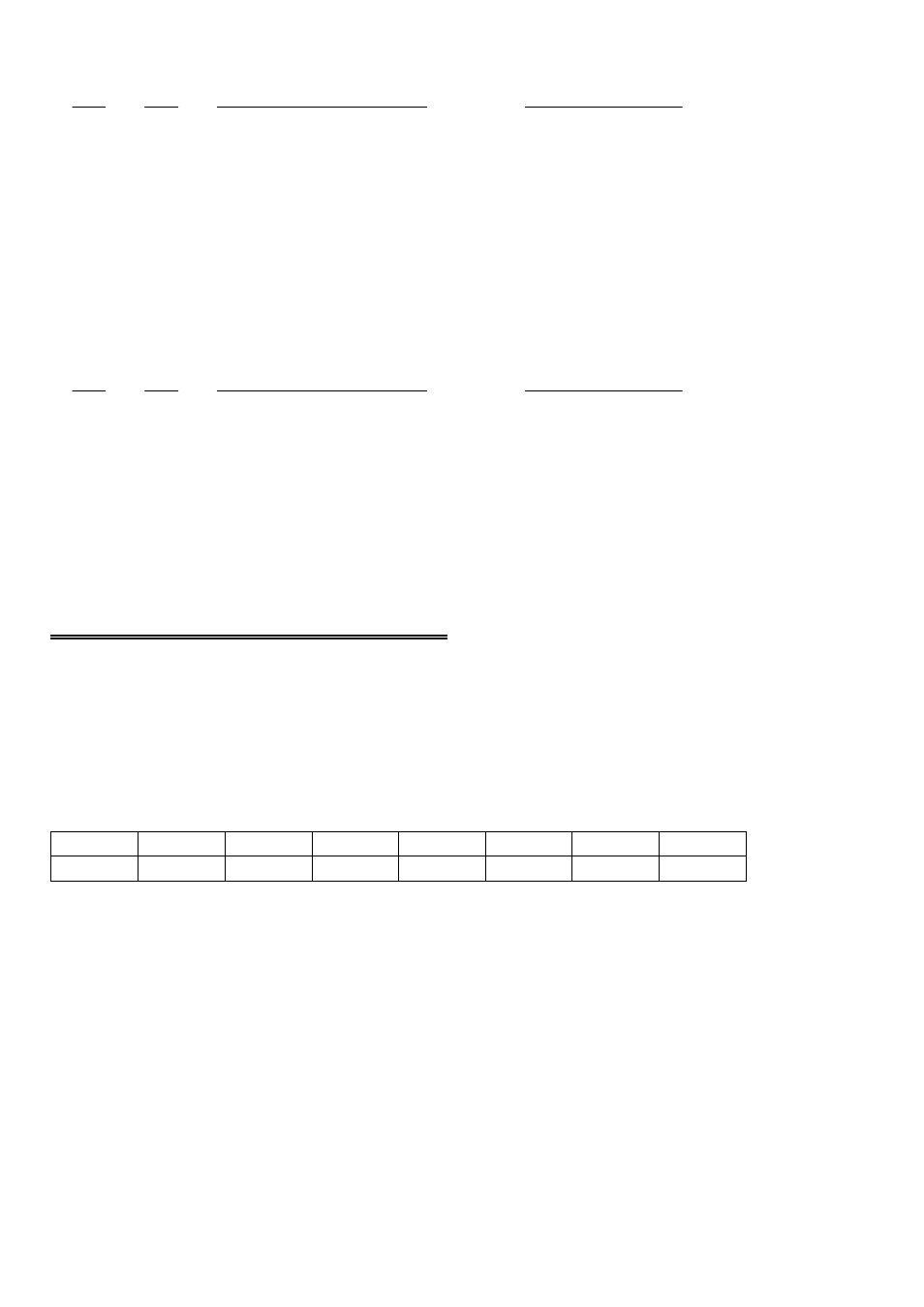
The numbers along the top row are the bit positions within the byte and the numbers
and symbols in the bottom row are the functions of each bit.
To write to or read from a register in decimal or HEX, the weights in Table 4-1 apply:
6