Digital input / output, Digital input / output -2 – Measurement Computing PCI-CTR10 User Manual
Page 15
PCI-CTR10 User's Guide
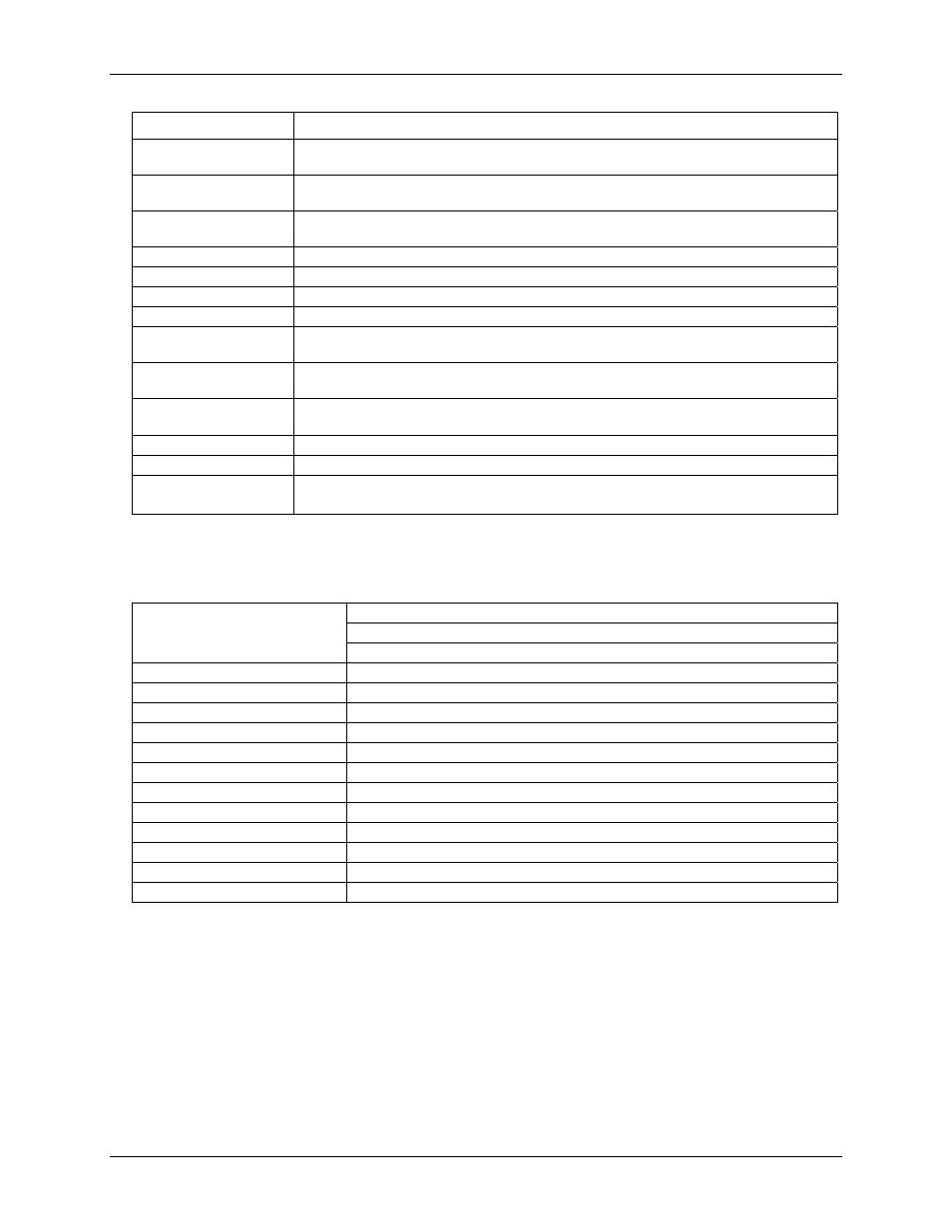
Specifications
Parameter Conditions
X2 clock frequency
scaler
BCD scaling (X2 divided by 10, 100, 1000 or 10000) or Binary scaling (X2 divided by 16,
256, 4096 or 65536)
High pulse width
(clock input)
70 ns min
Low pulse width
(clock input)
70 ns min
Gate width high
145 ns min
Gate width low
145 ns min
Input low voltage
-0.5 V min, 0.8 V max
Input high voltage
2.2 V min, Vcc max
Output low voltage @
IIl = 3.2 mA
0.4 V max
Output high voltage @
IIH = -200 µA
2.4 V min
Crystal oscillator
frequency
10 MHz
Frequency accuracy
50 ppm
Data transfer
Programmed I/O, interrupt
Power-up / reset state
CTRnOUT_x: low impedance
OSCOUT_x: enabled
Digital input / output
Table 2. Digital I/O specifications
Discrete, 5V/TTL compatible
Output:74ACT273
Digital type
Input: 74LS373
Number of I/O
8 input, 8 output per 37-pin D connector
Configuration, per connector
1 bank of 8 as output, 1 bank of 8 as strobed input
Input high voltage
2.0 V min, 7.0 V absolute max
Input low voltage
0.8 V max, –0.5 V absolute min
Output high voltage
3.94 volts min @ -24 mA (Vcc = 4.5 V)
Output low voltage
0.36 volts max @ 24 mA (Vcc = 4.5 V)
Data transfer
Programmed I/O
Power-up / reset state
Digital outputs power on and Reset to TTL low
Din Strobe
Active low latch enable input, internally pulled high through 10 Kohm resistor
Din Strobe pulse width high/low
15 nS min
Data setup to Din Strobe
5 nS min
Data hold from Din Strobe
20 nS min
4-2