Measurement Computing CIO-CTRxxHD User Manual
Page 11
5.2
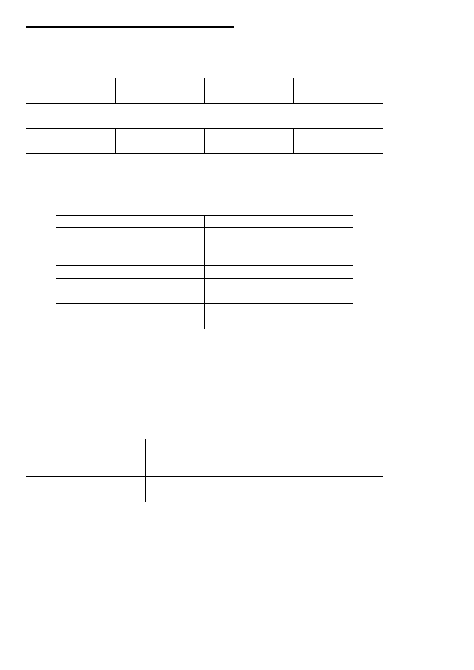
BASE +400 hex & BASE +401 hex
BASE + 400 controls the wait state for the board and the clock source and interrupt
level for 9513 #1 and 9513 #2
L0
L1
L2
CLK00
CLK01
CLK10
CLK11
WSEN
D0
D1
D2
D3
D4
D5
D6
D7
BASE +401 controls the clock source and interrupt level for 9513 #3 and 9513 #4
L0
L1
L2
CLK00
CLK01
CLK10
CLK11
X
D0
D1
D2
D3
D4
D5
D6
D7
Read - No read function for these registers.
Write - L0, L1, and L2 select IRQ as follows:
Table 5-2. IRQ Select Codes
7
1
1
1
6
0
1
1
5
1
0
1
4
0
0
1
3
1
1
0
2
0
1
0
N/A
1
0
0
N/A
0
0
0
IRQ
L0
L1
L2
For BASE +400, CLK0# selects the clock cource for 9513 #1 (the chip designated
“U1”), CLK1# selects the clock source for 9513 #2 (the chip designated “U2”)
For BASE +401, CLK0# selects the clock cource for 9513 #3 (the chip designated
“U3” for the CIO-CTR20HD”), CLK1# selects the clock source for 9513 #4 (the chip
designated “U4” for the CIO-CTR20HD).
Table 5-3. Clock-Select Codes
N/A
1
1
External
0
1
5 MHz
1
0
1 MHz
0
0
CLOCK SOURCE
CLK#0
CLK#1
7
- ACC-300 (7 pages)
- AI-EXP32 (20 pages)
- AI-EXP48 (19 pages)
- BTH-1208LS (30 pages)
- 6K-ERB08 (32 pages)
- BTH-1208LS Quick Start (4 pages)
- 6K-SSR-RACK08 (33 pages)
- BTH-1208LS-OEM (27 pages)
- CB-COM-Digital (68 pages)
- CB-7018 (68 pages)
- CB-7000 Utilities (44 pages)
- CB-7080D (74 pages)
- CB-COM-7033 (44 pages)
- CB-COM-7017 (72 pages)
- CB-COM-7024 (76 pages)
- CB-NAP-7000P (36 pages)
- CIO-DAC02/16 (16 pages)
- CIO-DAC02 (18 pages)
- CB-NAP-7000D (56 pages)
- CIO-DAC16-I (16 pages)
- CIO-DAC16/16 (20 pages)
- CIO-DAS08 (21 pages)
- CIO-DAC16 (20 pages)
- CIO-DAS08/JR (16 pages)
- CIO-DAS08/JR/16 (14 pages)
- CIO-DAS08/JR-AO (16 pages)
- CIO-DAS08-AOM (32 pages)
- CIO-DAS08-PGM (28 pages)
- CIO-DAS16/330 (34 pages)
- CIO-DAS48-I (17 pages)
- CIO-DAS16/M1 (38 pages)
- CIO-DAS48-PGA (18 pages)
- CIO-DAS800 (20 pages)
- CIO-DAS802/16 (22 pages)
- CIO-DAS6402/16 (40 pages)
- CIO-DAS-TEMP (20 pages)
- CIO-DDA06/16 (18 pages)
- CIO-DDA06/JR (17 pages)
- CIO-DIO24H (20 pages)
- CIO-DIO24/CTR3 (21 pages)
- CIO-DI192 (24 pages)
- CIO-DDA06 (21 pages)
- CIO-DIO48 (19 pages)
- CIO-DO192H (16 pages)
- CIO-DIO192 (20 pages)