P1 - analog i/o, Daqbook p1 pinout analog i/o – Measurement Computing 200 Series DaqBook User Manual
Page 27
DaqBook User’s Manual
01-23-02
DaqBook Hardware 3-9
DaqBook
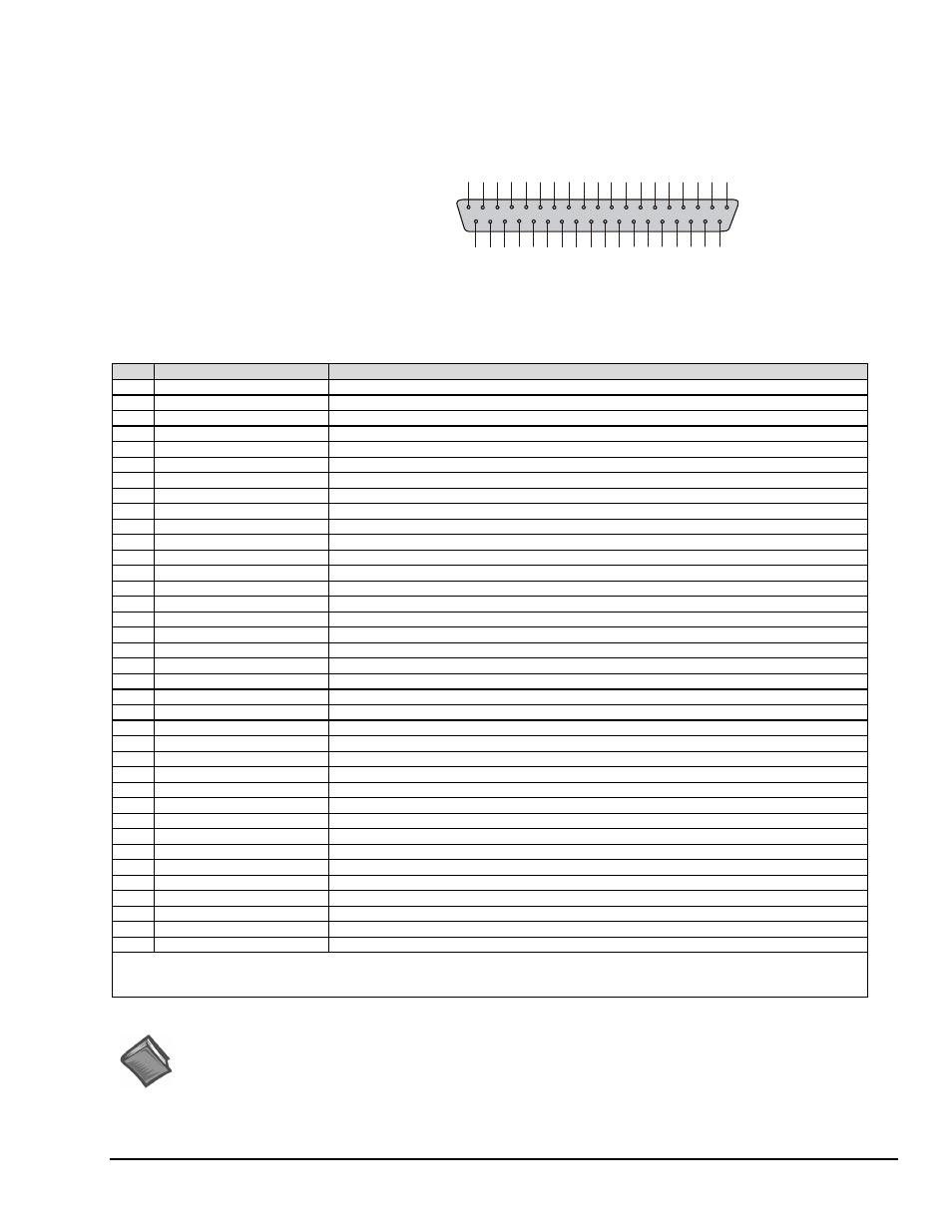
P1 Pinout
Analog I/O
(compatible with
Metrabyte DAS-16)
1
9
L
L
S
E
N
S
E
G
N
D
C
H
0
H
I
IN
3
7
C
H
1
H
I
IN
3
6
C
H
2
H
I
IN
3
5
C
H
3
H
I
IN
3
4
C
H
4
H
I
IN
3
3
C
H
5
H
I
IN
3
2
C
H
6
H
I
IN
3
1
C
H
7
H
I
IN
3
0
L
L
G
N
D
2
9
L
L
G
N
D
2
8
D
/A
1
O
U
T
2
7
S
S
H
/D
/A
1
R
E
F
I
N
2
6
IP
0
/T
R
IG
0
2
5
IP
2
/C
T
R
0
G
A
T
E
2
4
0
P
0
/C
H
S
0
2
3
0
P
2
/C
H
S
2
2
2
C
TR
0
C
LO
C
K
IN
/+
15
V
D
C
2
1
C
T
R
2
O
U
T
2
0
8
V
R
E
F
(
-5
V
)
7
P
O
W
E
R
G
N
D
6
IP
1
/G
S
0
5
IP
3
/G
S
1
4
O
P
1
/C
H
S
1
3
O
P
3
/C
H
S
3
2
C
T
R
0
O
U
T
/-
1
5
V
D
C
1
+
5
V
P
W
R
1
0
D
/A
0
R
E
F
I
N
9
D
/A
0
O
U
T
18
C
H
0
L
O
IN
/*
C
H
8
H
I I
N
17
C
H
1
L
O
IN
/*
C
H
9
H
I I
N
16
C
H
2
L
O
IN
/*
C
H
10
H
I I
N
15
C
H
3
L
O
IN
/*
C
H
11
H
I I
N
14
C
H
4
L
O
IN
/*
C
H
12
H
I I
N
13
C
H
5
L
O
IN
/*
C
H
13
H
I I
N
12
C
H
6
L
O
IN
/*
C
H
14
H
I I
N
11
C
H
7
L
O
IN
/*
C
H
15
H
I I
N
Pin
Signal Name
Description for P1 Pin Use
1
+5 PWR
+5 V supply
see Note 1
2
CTR 0 OUT/-15 VDC
Counter 0 output (8254 chip)/ -15 V supply
see Note 1
3
OP 3/CHS 3
Digital out bit 3/channel select line for expansion cards
4
OP 1/CHS 1
Digital out bit 1/channel select line for expansion cards
5
IP 3/GS 1
Digital in bit 3/gain select line for expansion cards
6
IP 1/GS 0
Digital in bit 1/gain select line for expansion cards
7
POWER GND
Digital ground
8
VREF (-5V)
-5 V supply @ 10 mA max
9
D/A 0 OUT
Digital to analog converter output ch 0
10
D/A 0 REF IN
Digital to analog converter reference in ch 0 (must invert)
11
CH 7 LO IN/CH 15 HI IN
Ch 7 LO IN (differential mode)/ch 15 HI IN (single-ended mode)
12
CH 6 LO IN/CH 14 HI IN
Ch 6 LO IN (differential mode)/ch 14 HI IN (single-ended mode)
13
CH 5 LO IN/CH 13 HI IN
Ch 5 LO IN (differential mode)/ch 13 HI IN (single-ended mode)
14
CH 4 LO IN/CH 12 HI IN
Ch 4 LO IN (differential mode)/ch 12 HI IN (single-ended mode)
15
CH 3 LO IN/CH 11 HI IN
Ch 3 LO IN (differential mode)/ch 11 HI IN (single-ended mode)
16
CH 2 LO IN/CH 10 HI IN
Ch 2 LO IN (differential mode)/ch 10 HI IN (single-ended mode)
17
CH 1 LO IN/CH 9 HI IN
Ch 1 LO IN (differential mode)/ch 9 HI IN(single-ended mode)
18
CH 0 LO IN/CH 8 HI IN
Ch 0 LO IN (differential mode)/ch 8 HI IN (single-ended mode)
19
L.L. GND
Low-level ground (analog ground - use with analog inputs and outputs)
20
CTR 2 OUT
Counter 2 output (8254 chip)
21
CTR 0 CLOCK IN/+15 VDC
Counter 0 clock in (8254 chip)/+15 V supply
see Note 1
22
OP 2/CHS 2
Digital output bit 2/ channel select line for expansion cards
23
OP 0/CHS 0
Digital output bit 0/channel select line for expansion cards
24
IP 2/CTR 0 GATE
Digital input bit 2/counter 0 gate (16-bit support only)
25
IP 0/TRIG 0
Digital input bit 0/trigger 0
26
D/A 1 REF IN/SSH
Digital-to-analog converter reference in ch 1 (must invert)/ SSH
27
D/A 1 OUT
Digital-to-analog converter output ch 1
28
L.L. GND
Low-level ground (analog ground - use with analog inputs and outputs)
29
L.L. GND
Low-level ground (analog ground - use with analog inputs and outputs)
30
CH 7 HI IN
Ch 7 HI IN (single-ended mode or differential mode)
31
CH 6 HI IN
Ch 6 HI IN (single-ended mode or differential mode)
32
CH 5 HI IN
Ch 5 HI IN (single-ended mode or differential mode)
33
CH 4 HI IN
Ch 4 HI IN (single-ended mode or differential mode)
34
CH 3 HI IN
Ch 3 HI IN (single-ended mode or differential mode)
35
CH 2 HI IN
Ch 2 HI IN (single-ended mode or differential mode)
36
CH 1 HI IN
Ch 1 HI IN (single-ended mode or differential mode)
37
CH 0 HI IN
Ch 0 HI IN (single-ended mode or differential mode)
Note: Software configuration commands determine P1 digital I/O pin functions. Actual shunt-jumper placement is required to provide
±15 VDC to expansion cards or disconnect internal DAC references to allow externally selected DAC references. Digital I/O cannot
be used with DBKs. “/” indicates the pin can be used for either function but not both at the same time.
Note 1: Refer to the
Power Management
section in the DBK options manual (p/n 457-0905).
Reference Note:
The
Power Management section of the DBK Option Cards and Modules User’s Manual
(p/n 457-0905) contains
additional power-related information. As a part of product support, this manual is automatically loaded onto your
hard drive during software installation. The default location is the Programs directory, which can be accessed
through the Windows Desktop.