Synchronized operations, Figure 9 – Measurement Computing USB-1608FS-Plus User Manual
Page 15
USB-1608FS-Plus User's Guide
Functional Details
15
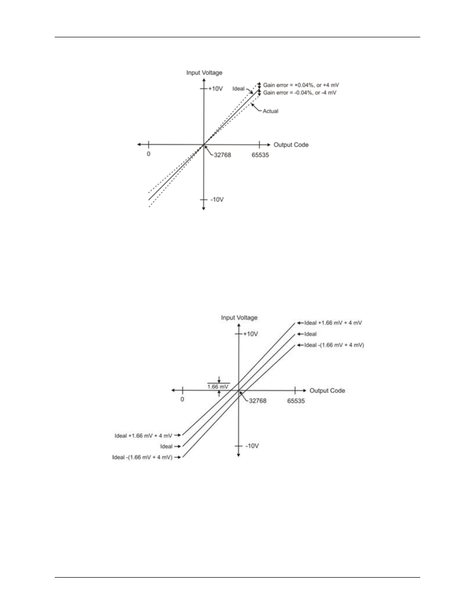
The accuracy plots in Figure 9 are drawn for clarity and are not drawn to scale.
Figure 9. ADC Transfer function with gain error
For example, a USB-1608FS-Plus exhibits a typical calibrated gain error of ±0.04% on all ranges. For the
±10 V range, this would yield 10 V × ±0.0002 = ±4 mV. This means that at full scale, neglecting the effect of
offset for the moment, the measurement would be within 4 mV of the actual value. Note that gain error is
expressed as a ratio. Values near ±FS (±10 V) are more affected from an absolute voltage standpoint than are
values near mid-scale, which see little or no voltage error.
Combining these two error sources in Figure 10, we have a plot of the error band at ±full scale (±10 V). This
plot is a graphical version of the typical accuracy specification of the product.
The accuracy plots in Figure 10 are drawn for clarity and are not drawn to scale.
Figure 10. Error band plot
Synchronized operations
You can connect the SYNC pin of multiple devices together in a master/slave configuration and acquire data
from the analog inputs of all devices using one clock.
When the SYNC pin is configured as an output, the internal A/D pacer clock signal is sent to the screw
terminal. You can output the clock to the SYNC pin of another device that is configured for A/D pacer input.