Pci-das1200 block diagram – Measurement Computing PCI-DAS1200 User Manual
Page 9
PCI-DAS1200 User's Guide
Introducing the PCI-DAS1200
8
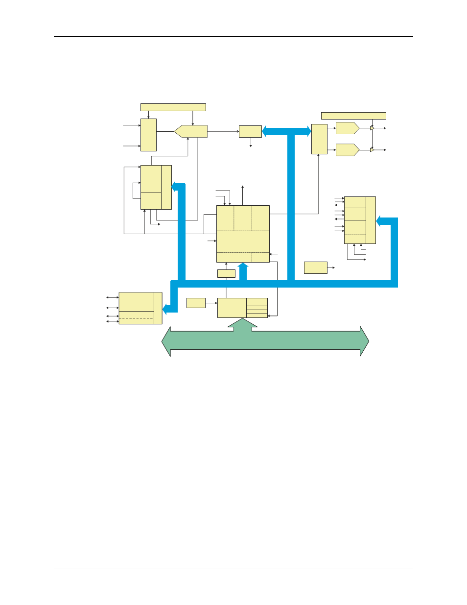
PCI-DAS1200 block diagram
PCI-DAS1200 functions are illustrated in the block diagram shown here.
Digital I/O
8
PCI
CONTROLLER
BADR1
BADR2
BADR3
BADR4
Interrupt
Boot
EEPROM
ADC
Pacer
Control
Scan
&
Burst
Logic
DAC
Control
Trigger
Control
Decode/Status
Int
Ctl
Bus
Timing
INT
Gains = 1, 2, 4, 8
XTRIG
CONTROLLER
FPGA
ADC
Pacer
CTR 2
CTR 1
Sample
Counter
CTR0
Co
nt
ro
l
Gain and Offset Autocal
INT
12-Bit, 330KHz
Mux
&
Gain
Analog In
16 CH S.E.
8 CH DIFF.
1024 x 12
FIFO
Gain and Offset Autocal
DAC
Data
Control
VDAC 0
VDAC 1
CTR1
ADC
Index
Counter
User
CTR 0
C
on
trol
Time Base
GATE
CLK
OUT
INT
XTRIG
Start EOC
DAC0
DAC1
12-bit, 10 uS
12-bit, 10 uS
INT
10 MHz
PCI Bus(5V, 32-bit, 33 MHZ)
Burst/Scan
Burst/Scan
EXT PCR
10 MHz
CTR2
CLK2
GATE2
OUT2
CLK1
GATE1
OUT1
FIRSTPORTA
FIRSTPORTB
Co
ntr
ol
FIRSTPORTCH
FIRSTPORTA(7:0)
FIRSTPORTB(7:0)
FIRSTPORTCH(3:0)
FIRSTPORTCL(3:0)
FIRSTPORTCL
Local Bus
PCI-DAS1200 and PCI-DAS1200/JR
block diagram
Figure 1. PCI-DAS1200 functional block diagram