Specifications, Analog input, Cold junction compensation – Measurement Computing CIO-EXP32 User Manual
Page 23: Chapter 5
Chapter 5
Specifications
Typical for 25 °C unless otherwise specified.
Specifications in italic text are guaranteed by design.
Analog input
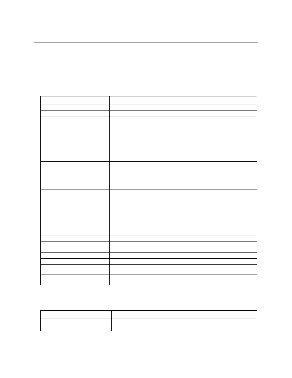
Table 1. Analog input specifications
Parameter
Specification
Number of channels
32 differential (2 banks of 16)
Input range
±10 V
Gain
Switch selectable by bank, additive values of X1, X10, X100, X200 and X500
Calibration
Two offset potentiometers per bank (16 channels) and one Cold Junction
Compensation adjustment potentiometer per board.
Gain error
Gain = 1
0.002% typical, 0.02% max
Gain = 10
0.005% typical, 0.05% max
Gain = 100
0.01% typical, 0.1% max
Gain = 200
0.02% typical, 0.2% max
Gain = 500
0.05% typical, 0.5% max
Non-linearity
Gain = 1
0.0005% typical, 0.005%
Gain = 10
0.001% typical, 0.01% max
Gain = 100
0.002% typical, 0.01% max
Gain = 200
0.003% typical, 0.01% max
Gain = 500
0.005% typical, 0.02% max
Temperature coefficient
Gain = 1
± 20 ppm / °C
Gain = 10
± 20 ppm / °C
Gain = 100
± 40 ppm / °C
Gain = 200
± 60 ppm / °C
Gain = 500
± 100 ppm / °C
Offset
± 15
µV / °C
Common mode range
±10 V
CMRR @ 60 Hz
90 dB
Input filter
7 Hz, selectable through solder bridge (C pad)
Open thermocouple detect
-50 mV at positive input when thermocouple is open, selectable through solder
bridge (V pad)
Input ground reference
100k ohms to ground, selectable through solder bridge (G pad)
Input leakage current
V and G pads open:
2 nA typical, 6 nA max
Input impedance
V and G pads open:
>100 Meg Ohms min
V and G pads shorted
100 k Ohms min
Absolute maximum input voltage
Power on:
±35 V
Power off:
±20 V
Cold junction compensation
Table 2. Cold junction compensation specifications
Parameter
Specification
CJC output voltage
24 mV / °C
CJC zero crossing
0 mV at 0 °C
23