0 control & data registers, 1 introduction – Measurement Computing CIO-DO24DD User Manual
Page 14
5.0 CONTROL & DATA REGISTERS
5.1 INTRODUCTION
CIO-DO24DD is a direct drive, 24-line digital switching board built up of logic chips.
There are n o configuration registers as su ch. There are on ly four (or eight) buffer
registers for holding the output values. The output circuits are capable of switching up
to 500 mA at up to 50V.
Each board is composed of parallel ou tput chips. Each address contains one latch
and one buffer controlling 8 output pins. The ports are arranged in sets of 3, with an
intervening unused address. This scheme allows partial compatibility with
applications written to control 82C55 based boards in w hich the 8 2C55 is used for
output only. On those boards every fourth address contains a configuration register.
The partial compatibility arises from the lack o f a read back of the output buffers on
the CIO-DO24DD or CIO-DO48DD.
To write control data to an o utput register, the individual bits must be set to 0 or 1
then combined to form a byte.
Table 5-1 has the register assignments for the CIO-DO24DD and CIO-DO48DD.
Note that the last four registers (Base + 4 to +7) apply only to the CIO-DO48DD.
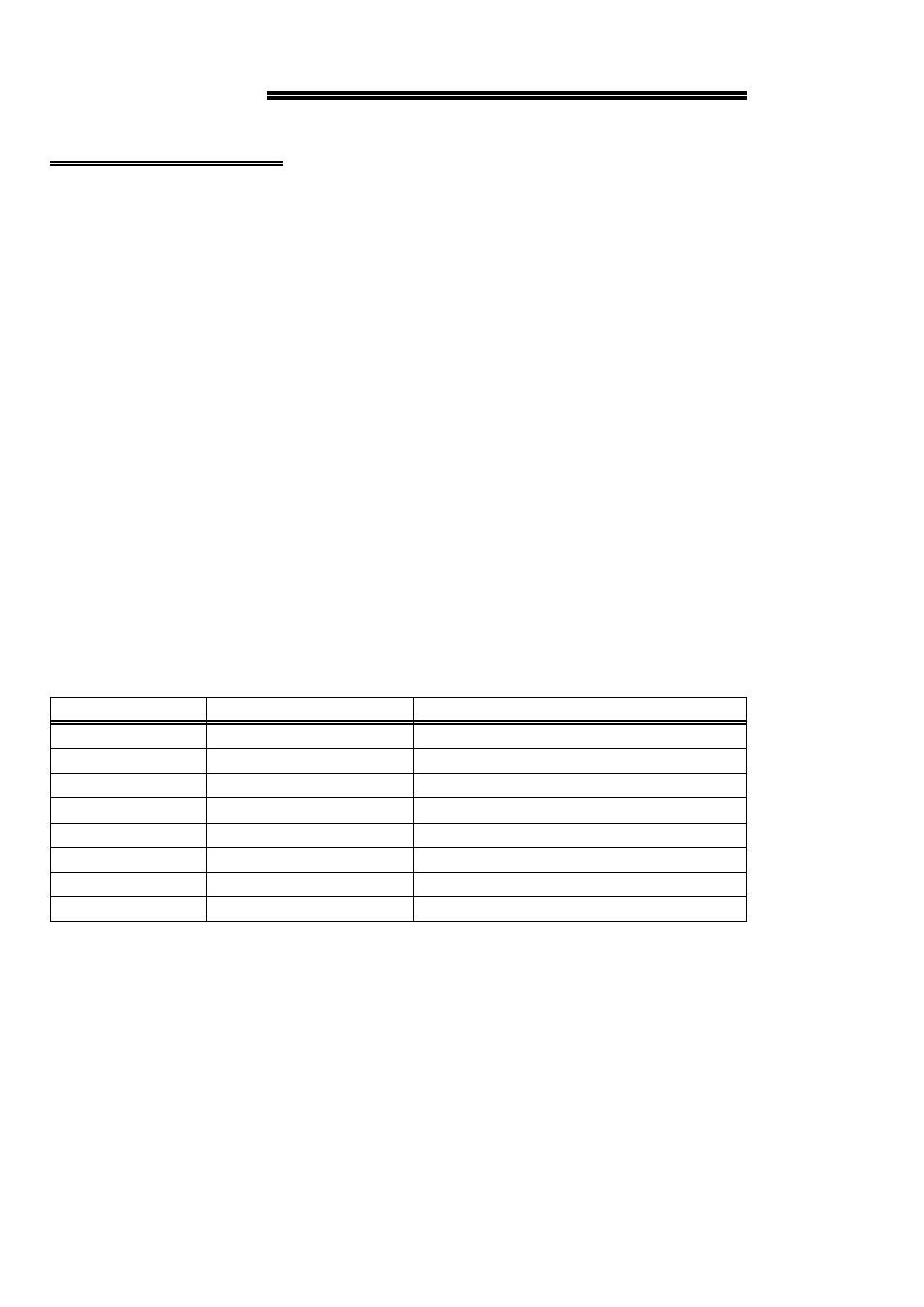
Table 5-1. Register Assignments
None
None
BASE + 7
Port 2C Outputs ( 48 bit model only)
None
BASE + 6
Port 2B Outputs ( 48 bit model only)
None
BASE + 5
Port 2A Outputs ( 48 bit model only)
None
BASE + 4
None
None
BASE + 3
Port 1C Outputs (24 & 48 bit models)
None
BASE + 2
Port 1B Outputs (24 & 48 bit models)
None
BASE + 1
Port 1A Outputs (24 & 48 bit models)
ID Code
BASE + 0
WRITE FUNCTION
READ FUNCTION
ADDRESS
Notice that the register layout is very similar to that of a standard 82C55 based digital
I/O board and the other high drive digital output boards. The alignment of ports A, B
& C are id entical and the position normally occupied by the configuration register is
left empty. This is so your existing digital board software will work without
modification.
10