Measurement Computing CIO-DAC16-I User Manual
Page 12
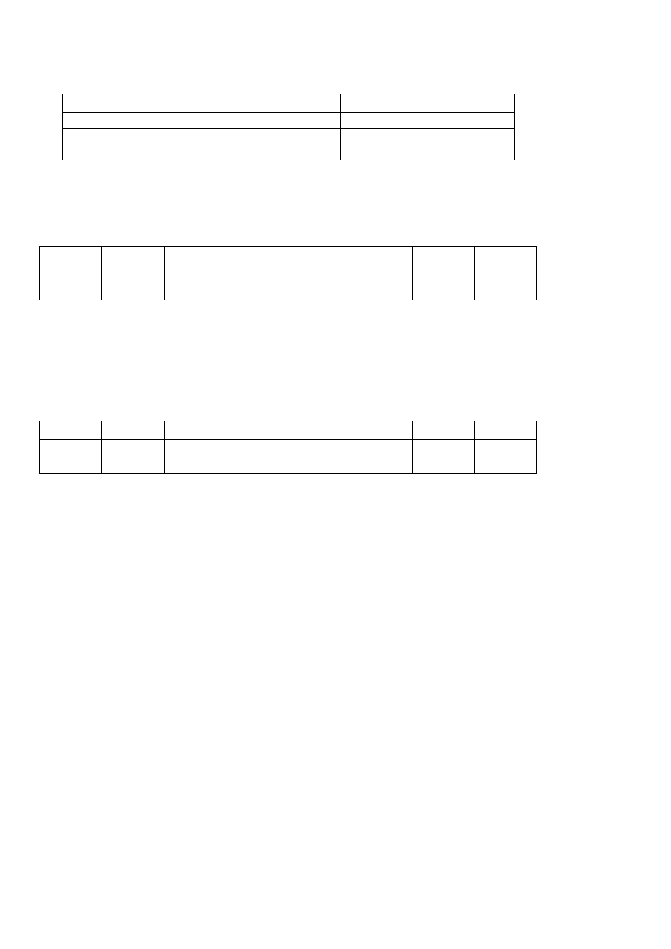
In summary form, the registers and their function are listed in the following table.
Table 4-2. Register Map
None
D/A Most Significant Nibble and
Channel address
BASE + 1
None
D/A Least Significant Byte
BASE + 0
READ FUNCTION
WRITE FUNCTION
ADDRESS
These two registers control all of the DACs on the CIO-DAC##-I. The first register,
BASE + 0, contains the least significant eight bits of D/A code and is written first.
BASE + 0
D12
(LSB)
D11
D10
D9
D8
D7
D6
D5
0
1
2
3
4
5
6
7
The second register contains the most significant four bits of D/A code and the four
bits that determine which channel the data will be sent to. This register is written to
second. A write to this register updates the output of the selected D/A with all 12
bits of the D/A code contained in the two registers.
BASE + 1
D4
D3
D2
D1
(MSB)
CH0
CH1
CH2
CH3
0
1
2
3
4
5
6
7
D12: 1 Data bits
CH3:0 Channel value (0000 = channel 0, 0101 = channel 5, etc.)
Updating the output of a particular DAC channel is a matter of calculating the code
for the output value desired and combining it with the channel number.
To calculate the data code, you first select the output you desire, then apply a
transfer function to that value. The transfer function for code = output is:
FSI / 4095 * CODE = Current Out +4 mA or CODE = Current Out - 4 / 16 * 4095
Full scale current (FSI) is not 20 mA, it is 20 - 4 or 16 mA. Use this in the equation
above.
For Example:
If CODE = 0, current output = 4 mA
If CODE = 4095, current output = 20 mA
8