Comtech EF Data UB-530 User Manual
Page 22
Breakout Panel
Revision 2
Connectors and Switches
MN/UB530.IOM
2–10
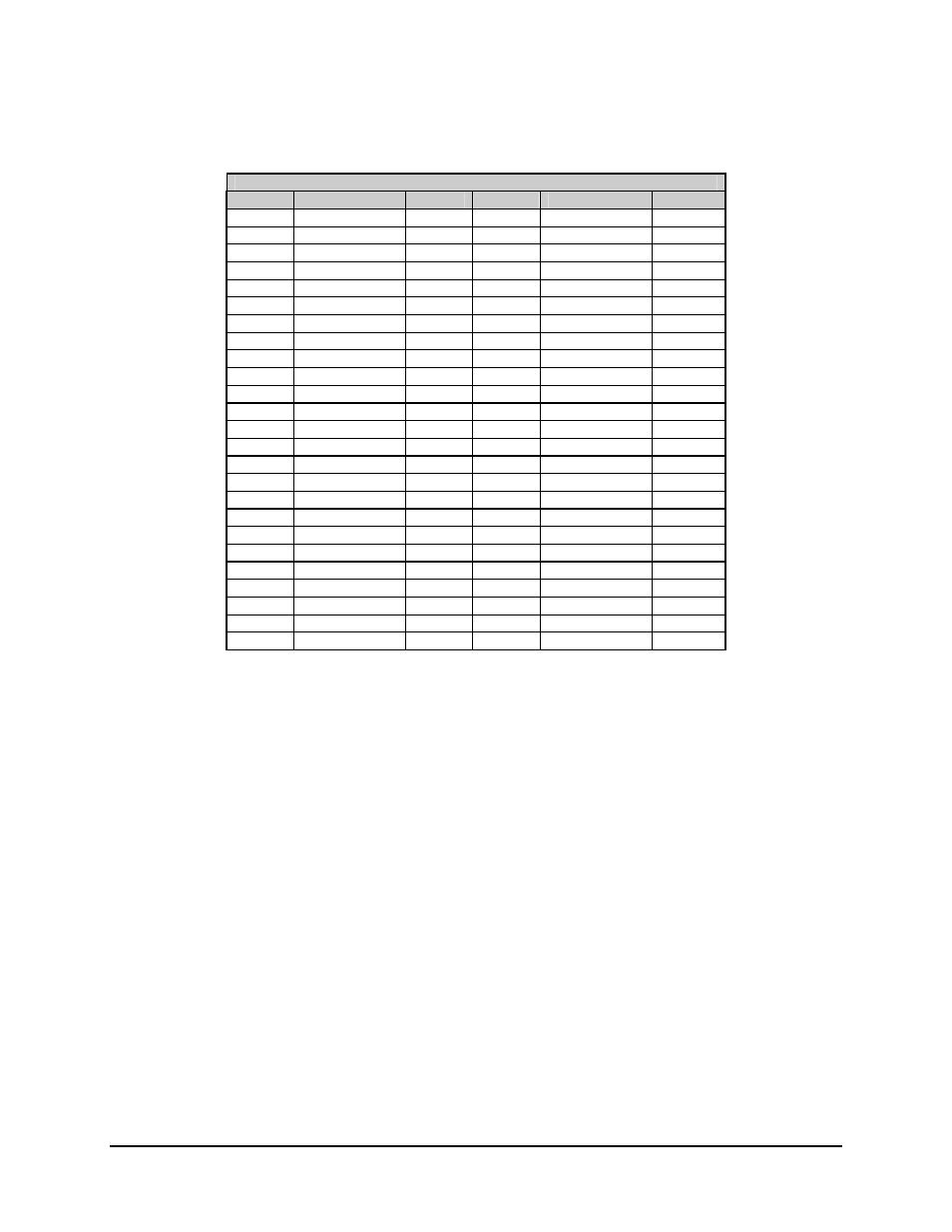
Table 2-3. Adapter Pinout For UB-530 To UB-300 Connection
25-Pin D Connector
Pin #
V.35 (RS-530)
To
Pin #
V.35 (UB-300)
Notes
1 SHLD 1 SHLD
2 SD-A
14 SD-A
3 RD-A
16 RD-A
4 RTS-A 4 RTS
5 CTS-A 5 CTS
6 DSR-A 6 DSR
7 SIGGND 7 SIGGND
8 RLSD-A 8 RLSD
9 SCR-B 17 SCR-B
10 RLSD-B 10
1
11 SCTE-B 24 SCTE-B
12 SCT-B 15 SCT-B
13 CTS-B 13
1
14 SD-B 2 SD-B
15 SCT-A 18 SCT-A
16 RD-B 3 RD-B
17 SCR-A 19 SCR-A
18
11
19 RTS-B 9
1
20 MC-A 22
MC-A
(EXC-A)
2
21 DF
21 DF 3
22 DSR-B 12
1
23 MC-B 23
MC-B
(EXC-B)
2
24 SCTE-A 25 SCTE-A
25 MF
20 MF 3
Notes:
1. These signals are used for RS-530 (RS-422) and not required for V.35 which
uses only the “A” side of the signals.
2. Use the MASTER (MC or EXC) clock for EXTERNAL clock input. This clock
input should equal the data rate unless the Asymmetrical Loop Timing Option
(ASLT) is available. The ASLT option allows selection of different clock rates
that vary from the digital data rate. Refer to the Utility/Modem Type/Modem
Options menu for the ASLT option information.
3. MF and DF are fault indication signals from the modem and are not V.35 or
RS-530 standard signals.