8 insert data output (j8), 9 external reference clock (j9), 10 esc channel (j10) – Comtech EF Data D&I User Manual
Page 21

D&I
Revision 0
Connectors ans Switches
MN/D-I.IOM
2–9
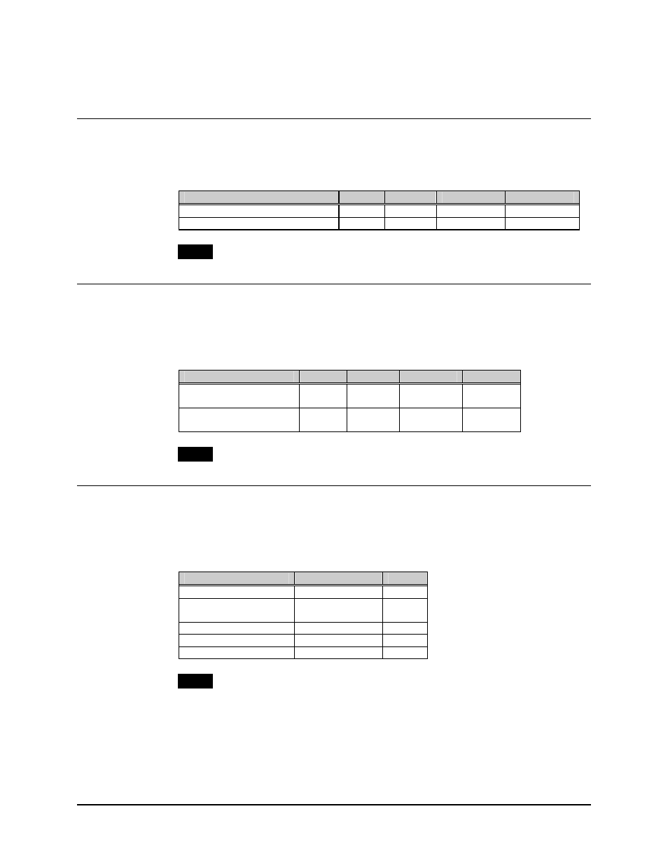
2.8 Insert Data Output (J8)
The unbalanced and balanced insert data output connection is a BNC connector located at
the front of the breakout panel. For J8 selections, use S2 located at the rear of the panel.
Signal Function
Name
Switch
Switch #
Position
Unbalanced Insert Data Output
IDO
S2
5, 6/7, 8
OFF/ON
Balanced Insert Data Output
IDO
S2
5, 6/7, 8
ON/OFF
NOTE
S2 is ON in the down position (toward PCB).
2.9 External Reference Clock (J9)
The unbalanced and balanced external reference clock input is a BNC connector located
at the front of the breakout panel. For J9 selections, use S3, located at the rear of the
panel.
Signal Function
Name
Switch
Switch #
Position
Unbalanced External
Reference Clock
EXC
S3
1, 3/2, 4
OFF/ON
Balanced External
Reference Clock
EXC
S3
1, 3/2, 4
ON/OFF
NOTE
S3 is ON in the down position (toward PCB).
2.10 ESC Channel (J10)
The ESC Channel interface is a 25-pin female D connector located at the front of the
breakout panel. Screw locks are provided for mechanical security of the mating
connector.
Signal Function
Name
Pin #
Ground GND
1,
7
Terrestrial Tx Data
Terrestrial Rx Data
TER–TXDAT
TER–RXDAT
2
3
Request To Send
RTS
4
Clear To Send
CTS
5
Data Set Ready
DSR
6
NOTE
RTS and CTS are looped together on the connector.
