5 drop data input (j5), 6 drop data output (j6), 7 insert data input (j7) – Comtech EF Data D&I User Manual
Page 20
D&I
Revision 0
Connectors ans Switches
MN/D-I.IOM
2–8
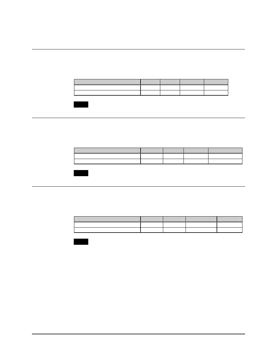
2.5 Drop Data Input (J5)
The unbalanced and balanced drop data input connection is a BNC connector located at
the front of the breakout panel. For J5 selections, use S1 located at the rear of the panel.
Signal Function
Name
Switch
Switch #
Position
Unbalanced Drop Data Input
DDI
S1
1, 2/3, 4
ON/OFF
Balanced Drop Data Input
DDI
S1
1, 2/3, 4
OFF/ON
NOTE
S1 is ON in the down position (toward PCB).
2.6 Drop Data Output (J6)
The unbalanced and balanced drop data output connection is a BNC connector located at
the front of the breakout panel. For J6 selections, use S1 located at the rear of the panel.
Signal Function
Name
Switch
Switch #
Position
Unbalanced Drop Data Output
DDO
S1
5, 6/7, 8
OFF/ON
Balanced Drop Data Output
DDO
S1
5, 6/7, 8
ON/OFF
NOTE
S1 is ON in the down position (toward PCB).
2.7 Insert Data Input (J7)
The unbalanced and balanced insert data input connection is a BNC connector located at
the front of the breakout panel. For J7 selections, use S2 located at the rear of the panel.
Signal Function
Name
Switch
Switch #
Position
Unbalanced Insert Data Input
IDI
S2
1, 2/3, 4
OFF/ON
Balanced Insert Data Input
IDI
S2
1, 2/3, 4
ON/OFF
NOTE
S1 is ON in the down position (toward PCB).