Aplex Technology AHM-6057A User Manual
Page 42
AHM-6XX7A User Manual
42
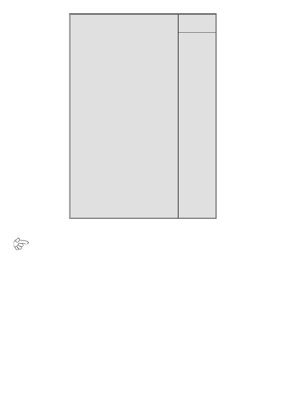
DRAM Timing Selectable [By SPD]
Item Help
X
CAS Latency Time Auto
X
DRAM RAS# to CAS# Delay Auto
Menu Lev
el►
X
DRAM RAS# Precharge Auto
X
Precharge Delay (tRAS) Auto
X
System Memory Frequency Auto
SLP_S4# Assertion Width [1 to 2
Sec.]
System BIOS Cacheable [Enabled]
Video BIOS Cacheable [Disabled]
Memory Hole At 15M-16M [Disabled]
►PCI Express Root Port Func [Press
Enter]
** Onboard VGA Setting **
On-Chip Frame Buffer Size [ 8MB]
DVMT Mode [DVMT]
DVMT/Fixed Memory Size [128MB]
Boot Display [VBIOS
Default]
LCD Panel Type [LVDS1 18 1024 X
768]
LCD Panel Brightness [Level 8]
↑↓→←:Move Enter:Select +/-/PU/PD:Value F10:Save ESC:Exit F1:General Help
F5: Previous Values F6: Fail-Safe Defaults F7: Optimized Defaults
Note: If you are not familiar with chipset, never modify these settings at will.
DRAM Timing Selectable
Two options are available.
Manual (Manual setup)
By SPD (DRAM timing is set automatically according to memory SPD data)
When selecting Manual, the following five items are configurable; when selecting By SPD, the
following five items are not configurable.
CAS Latency Time
Once a SDRAM is installed, the clock latency will be determined by DRAM clock settings. The
options are: 5, 4, 3 and Auto.
DRAM RAS-to-CAS Delay
You may set the delay period between CAS and RAS signal for DRAM read & write or refreshing.