Dip switch debug port, Dip switch, Debug port – NEXCOM PEAK 887VL2 User Manual
Page 35
Copyright © 2013 NEXCOM International Co., Ltd. All Rights Reserved.
21
PEAK 887VL2 User Manual
Chapter 2: Jumpers and Connectors
O N
1 2
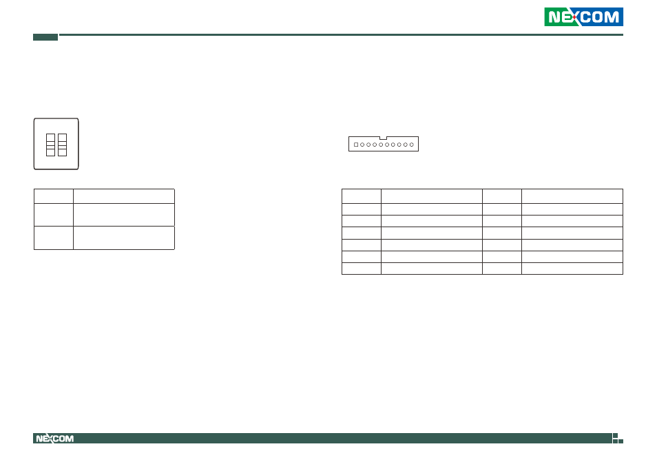
DIP Switch
Connector type: 2x2 4-pin DIP switch
Connector location: SW1
Debug Port
Connector type: 1x10 10-pin header, 1.0mm pitch
Connector location: J4
Pin
Description
SW1.1
ON: Control by backplan
OFF: Control by SW1.2
SW1.2
ON: PCIe x1
OFF: PCIe x4
Pin
Definition
Pin
Definition
1
GND
2
RST_SIO_N
3
CLK_PCI_P80
4
LPC_FRAME#
5
LPC_AD3
6
LPC_AD2
7
LPC_AD1
8
LPC_AD0
9
VCC3
10
VCC3
MH1
GND
MH2
GND
1
10
See also other documents in the category NEXCOM Hardware:
- EBC 352 (68 pages)
- EBC 353 (62 pages)
- EBC 355 (63 pages)
- EBC 354 (63 pages)
- ICES 268 (96 pages)
- ICES 667 (100 pages)
- ICES 254 (98 pages)
- NEX 604 (61 pages)
- NEX 608 (67 pages)
- ICES 668 (105 pages)
- NEX 607 (75 pages)
- NEX 609 (61 pages)
- NEX 611 (51 pages)
- NEX 613 (45 pages)
- NEX 617 (53 pages)
- NISE 101 (79 pages)
- NISE 104 (78 pages)
- NISE 2020 (84 pages)
- NISE 105A (78 pages)
- NISE 103 (83 pages)
- NISE 2110A (87 pages)
- NISE 2420 (84 pages)
- NISE 301 (74 pages)
- NISE 2310E (107 pages)
- NISE 2210E (110 pages)
- NISE 3100eP2 (75 pages)
- NISE 300 (95 pages)
- NISE 3140P2E (88 pages)
- NISE 3520P2E (125 pages)
- MAC 3500P2-GTS8 (120 pages)
- NISE 3600E (102 pages)
- NISE 3720P2E (85 pages)
- NISE 3640P2E (105 pages)
- NISE 3640M2E (108 pages)
- NISE 4000 (102 pages)
- nTUF 600 (100 pages)
- NEX 716VL2G (71 pages)
- NISE 4000P4E (128 pages)
- NISE 4000P2E (131 pages)
- NEX 732L2G (71 pages)
- NEX 883 (53 pages)
- NEX 890 (58 pages)
- NEX 980 (52 pages)
- NEX 852VL2 (62 pages)
- NEX 981 (47 pages)