Specifications, Resistance measurement, Measurement – Elenco Digital Mulitmeter Kit User Manual
Page 16: Figure 7, Figure 8, Figure 8 shows a simplified diagram of the h, Of the transistor, Diode check, Transistor h, Test
DIODE CHECK
RANGE
RESOLUTION
MAX TEST CURRENT
MAX OPEN CIRCUIT VOLTAGE
DIODE
1mV
1.4mA
2.8V
TRANSISTOR h
FE
TEST
RANGE
TEST RANGE
TEST CURRENT
TEST VOLTAGE
NPN/PNP
0 - 1000
Ib = 10
μ
A
Vce 3V
-15-
SPECIFICATIONS
GENERAL
DISPLAY
3 1/2 digit LCD, with polarity
OVERRANGE INDICATION
3 least significant digits blanked.
MAXIMUM COMMON MODE
VOLTAGE
500V peak.
STORAGE ENVIRONMENT
–15
O
C to 50
O
C.
TEMPERATURE COEFFICIENT
(0
O
C to 18
O
C and 28
O
C to 50
O
C)
less than 0.1 x applicable accuracy
specification per
O
C.
POWER
9V alkaline or carbon zinc battery.
DIMENSIONS
128 x 75 x 24mm.
DC VOLTAGE
RANGE
RESOLUTION
ACCURACY
200mV
0.1mV
+0.5% rdg + 2d
2V
1mV
+0.5% rdg + 2d
20V
10mV
+0.5% rdg + 2d
200V
100mV
+0.5% rdg + 2d
1000V
1V
+0.5% rdg + 2d
MAXIMUM ALLOWABLE INPUT
1000VDC or peak AC.
INPUT IMPEDANCE
1M
Ω
.
DC CURRENT
RANGE
RESOLUTION
ACCURACY
200
μ
A
0.1
μ
A
+1.8% rdg + 2d
2mA
1
μ
A
+1.8% rdg + 2d
20mA
10
μ
A
+1.8% rdg + 2d
200mA
100
μ
A
+2% rdg + 2d
10A
10mA
+2% rdg + 3d
OVERLOAD PROTECTION
.2A/250V fuse (mA input only).
AC VOLTAGE
RANGE
RESOLUTION
ACCURACY
200V
100mV
+2% rdg + 10d
750V
1V
+2% rdg + 10d
MAXIMUM ALLOWABLE INPUT
750Vrms.
FREQUENCY
50 - 500Hz.
RESISTANCE
RANGE
RESOLUTION
ACCURACY
200
Ω
0.1
Ω
+1% rdg + 10d
2k
Ω
1
Ω
+1% rdg + 10d
20k
Ω
10
Ω
+1% rdg + 10d
200k
Ω
100
Ω
+1% rdg + 10d
2000k
Ω
1k
Ω
+1% rdg + 4d
MAXIMUM OPEN CIRCUIT VOLTAGE
2.8V.
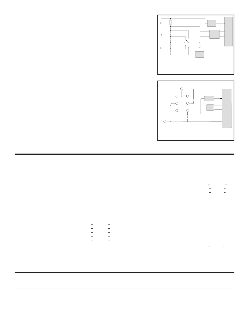
RESISTANCE MEASUREMENT
Figure 7 shows a simplified diagram of the resistance measurement
function. A simple series circuit is formed by the voltage source, a
reference resistor from the voltage divider (selected by the selector
switches), and the test (unknown) resistor. The ratio of the two resistors
is equal to the ratio of their respective voltage drops. Therefore, since
the value of one resistor is known, the value of the second can be
determined by using the voltage drop across the known resistor as a
reference. This determination is made directly by the A/D converter.
Overall operation of the A/D converter during a resistance
measurement is basically as described earlier with one exception. The
reference voltage present during a voltage measurement is replaced by
the voltage drop across the reference resistor. This allows the voltage
across the unknown resistor to be read during the read period.
h
FE
MEASUREMENT
Figure 8 shows a simplified diagram of the h
FE
measurement function.
Internal circuits in the 7106 IC maintain the COMMON line at 2.8 volts
below V+. When a PNP transistor is plugged into the transistor socket,
base to emitter current flows through resistor R1. The voltage drop in
resistor R1 due to the collector current is fed to the 7106 and indicates
the h
FE
of the transistor. For an NPN transistor, the emitter current
through R2 indicates the h
FE
of the transistor.
Figure 7
Simplified Resistance Measurement Diagram
Ω
900k
Ω
Test
Resistor
100
Ω
900
Ω
2000
Ω
/Dio
200
Ω
7106
Reference
Voltage
Low Pass
Filter
Voltage
Source
Common
90k
Ω
9k
Ω
2000k
Ω
20k
Ω
200k
Ω
Figure 8
R1
Common
R3
R2
PNP
NPN
7106
100mV
Ref.
Low Pass
Filter
V+
E
C
C
E
B
B