Assemble components to the pc board, Figure g, Figure 3 figure 4a figure 4c figure 4b – Elenco AutoScan Fm Radio Kit User Manual
Page 7: R install speaker, R install battery holder, Equivalent schematic and connection diagrams, Dual-in-line and small outline packages, Step 1 step 2 step 3 step 4
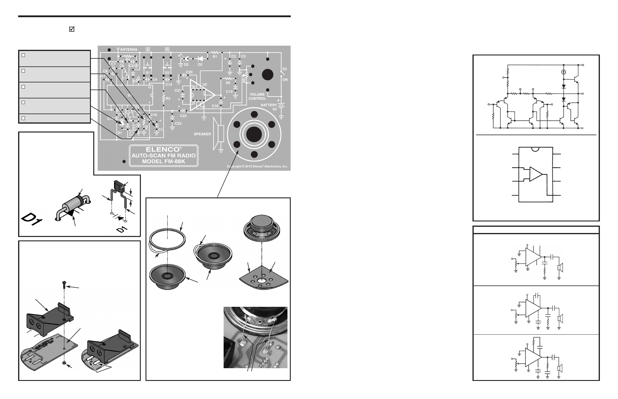
Figure G
Your kit contains one of two types of
varactor. Use the figure that
corresponds to your varactor style
for mounting instructions.
Mount the varactor flush to the PC
board with the printed band in the
same direction as marked. Solder
and cut off excess leads.
transferred through resistor R3 to the anode of the
varactor diode D1 (BB910), causing its capacitance
to decrease. Decreasing the capacitance of D1
increases the frequency of the local Oscillator (VCO).
The Oscillator voltage and signals of all the other FM
stations (Fs) from pin 11 are inputted into the Mixer.
The output of the mixer is only FM signals whose
frequencies are equal to the differences of the
oscillator and the original station frequency.
Only a signal whose carrier frequency is equal to
IF can reach the “Demodulator”. Selectivity (ability
to “pick out” one station while rejecting all others)
is accomplished by two active filters made from the
capacitors connected to pins 6, 7, 8, 9 and 10). The
oscillator frequency increases until the condition
Fo – Fs = 70kHz is accomplished. When this
happens, the charging of the capacitor is halted by
the command that is sent into the “Tuning Search”
circuit by two detectors (diode-blocks) located in
the “Mute Control” circuit.
In order to hold the frequency, the voltage on pin 16
must not change until the “Scan” switch is pushed
again. That is the function of the AFC (Automatic
Frequency Control) circuit; controlling the voltage on
pin 16.
When the switch S2 “R” (Reset) is pushed, the
capacitor C14 is discharged, the voltage on pin 16
drops down to zero, and the receiver is set to the low
end of the reception bandwidth 88MHz.
Capacitor C23 and resistor R2 filter out the radio
frequency component of the signal, leaving a clean
audio signal. Capacitor C22 couples the audio signal
to the input of the power amplifier. Since the
maximum operating DC voltage of the U1 is 5V, the
battery voltage must be regulated down.
Components D2, D3, R1, C1, C17 and C* make up
that circuit.
Our kit uses the standard design for the audio amplifier
on base of the integrated circuit (U2) LM-386, or
identical. In Figure 3, you can see equivalent schematic
and connection diagrams. To make the LM-386 a more
versatile amplifier, two pins (1 and 8) are provided for
gain control. With pins 1 and 8 open, the 1.35k
Ω
resistor sets the gain at 20 (see Figure 4a). The gain
will go up to 200 (see Figure 4b) if a capacitor
(capacitor C21) is placed between pins 1 and 8. The
gain can be set to any value from 20 to 200 if resistor
is placed in series with the capacitor. The amplifier with
a gain of 150 is shown in Figure 4c. The amount of gain
control is varied by potentiometer R6, which also varies
the audio level and, consequently, the volume.
Capacitor C20 is a bypass and necessary for an
amplifier with a high gain IC. Capacitor C18 blocks the
DC to the speaker while allowing the AC to pass.
-6-
Figure 3
Figure 4a
Figure 4c
Figure 4b
Typical Applications
Amplifier with Gain = 20
Minimum Parts
V
IN
V
S
2
6
1
8
5
7
4
LM386
+
+
–
.05
μ
F
10
Ω
10k
Ω
Amplifier with Gain = 150
Amplifier with Gain = 200
3
V
IN
V
S
2
6
1
8
5
7
4
LM386
+
–
10k
Ω
3
+
.05
μ
F
10
Ω
BYPASS
+
10
μ
F
V
IN
V
S
2
6
1
8
5
7
4
LM386
+
–
10k
Ω
3
.05
μ
F
10
Ω
BYPASS
47
Ω
10
μ
F
+
+
Equivalent Schematic and Connection Diagrams
V
OUT
V
S
6
5
7
4
15k
Ω
BYPASS
GND
15k
Ω
2
– INPUT
150
Ω
1.35k
Ω
8
GAIN
1
GAIN
15k
Ω
50k
Ω
50k
Ω
+ INPUT
Dual-In-Line and Small Outline Packages
Top View
GAIN
– INPUT
+ INPUT
GND
GAIN
BYPASS
V
S
V
OUT
4
1
2
3
5
8
7
6
3
-9-
r Install speaker
Pad
Backing
Speaker
Backing
Step 1
Step 2
Step 3
Step 4
PC board
(foil side)
Step 1:
If the speaker pad has
center and outside pieces, then
remove them. Peel the backing
off of one side of the speaker
pad and stick the pad onto the
speaker.
Step 2:
Remove the other
backing from the speaker pad.
Step 3:
Stick the speaker onto
the solder side of the PC board.
Step 4:
Solder two 1½” wires
from the speaker to the pads
+SP and –SP.
ASSEMBLE COMPONENTS TO THE PC BOARD
Place a check mark in the box provided next to each step to indicate that the step is completed.
C1 - 100
μ
F, Electrolytic
(see Figure D)
R2 - 18k
Ω
5% 1/4W Res.
(brown-gray-orange-gold)
C13 - 680pF Discap
(681 or 680)
D1 - BB909/BB910 Varactor
(see Figure G)
C17 - 0.1
μ
F Discap (104)
r Install battery holder
Bend the leads of the battery holder as shown.
Fasten the battery holder to the PC board with a
M1.8 x 7.5mm screw and M1.8 nut. Solder the leads
to the PC board pads as shown.
Battery holder
M1.8 Nut
M1.8 x 7.5mm Screw
Foil side of
PC board
Solder
Printed band
PC board marking
1½” wires
Beveled
edge
0.3”
0.05”
+
Outer edge of
PC board
-OR-