Table 1-9, D-sub 9p com pin assignment, Table 1-10 – ADLINK MXE-5400 User Manual
Page 30: Digital i/o specifications, Preliminary
PRELIMINARY
18
Introduction
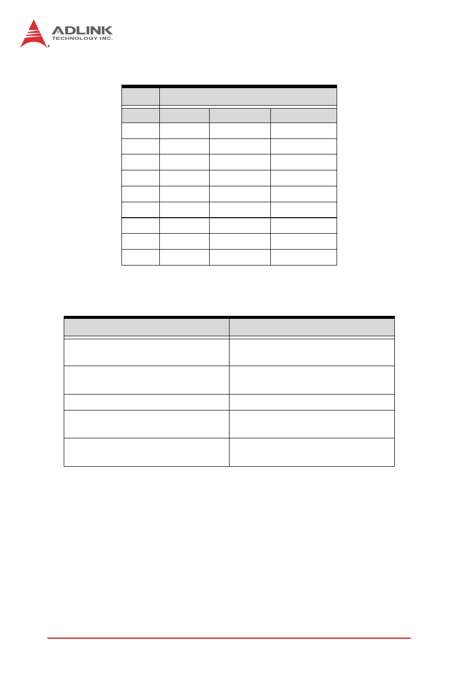
Table 1-9: D-SUB 9P COM Pin Assignment
Table 1-10: Digital I/O Specifications
Pin
Signal
RS-232
RS-422
RS-485
1
DCD#
TXD422-
485DATA-
2
RXD
TXD422+
485DATA+
3
TXD
RXD422+
N/C
4
DTR#
RXD422-
N/C
5
GND
N/C
N/C
6
DSR#
N/C
N/C
7
RTS#
N/C
N/C
8
CTS#
N/C
N/C
9
RI#
N/C
N/C
8CH Isolated DI
8CH Isolated DO
Logic high: 5 to 24 V
Output: Open Drain N- Channel
Power MOSFET driver
Logic low: 0 to 1.5 V
250 mA for all channels @ 60°C,
100% duty
Input resistance: 8.2 k @ 0.5 W
Supply voltage: 5 to 35 VDC
Interrupt source: DI
Isolation voltage: 1.5KV DC
channel 0 to 7
Isolation voltage: 1.5KV DC
channel 0 to 7
200 mA for +V5DIO_ISO (max)
See also other documents in the category ADLINK Hardware:
- USB-1901 (84 pages)
- USB-1210 (54 pages)
- USB-2401 (60 pages)
- USB-7230 (50 pages)
- USB-2405 (56 pages)
- DAQe-2010 (92 pages)
- DAQe-2204 (100 pages)
- DAQe-2213 (94 pages)
- DAQe-2501 (74 pages)
- PXI-2010 (84 pages)
- PXI-2020 (60 pages)
- PXI-2501 (62 pages)
- cPCI-9116 (98 pages)
- ACL-8112 Series (94 pages)
- ACL-8112 Series (92 pages)
- ACL-8112 Series (93 pages)
- ACL-8216 (75 pages)
- ACL-8111 (61 pages)
- PCM-9112+ (10 pages)
- PCM-9112+ (94 pages)
- cPCI-6216V (47 pages)
- ACL-6126 (28 pages)
- ACL-6128A (40 pages)
- PCM-6308V+ (52 pages)
- PCM-6308V+ (4 pages)
- PCI-7444 (82 pages)
- PCI-7434 (48 pages)
- PCI-7234 (56 pages)
- PCI-7260 (66 pages)
- PCI-7258 (38 pages)
- PCI-7256 (48 pages)
- PCI-7250 (48 pages)
- LPCI-7250 (48 pages)
- PCI-7396 (65 pages)
- PCI-7296 (59 pages)
- PCI-8554 (67 pages)
- PCIe-7360 (94 pages)
- PCIe-7350 (86 pages)
- PCIe-7300A (114 pages)
- PCIe-7200 (51 pages)
- PCI-7300A (112 pages)
- PCI-7300A (83 pages)
- PCI-7200 (96 pages)
- cPCI-7300 (83 pages)
- cPCI-7300 (82 pages)