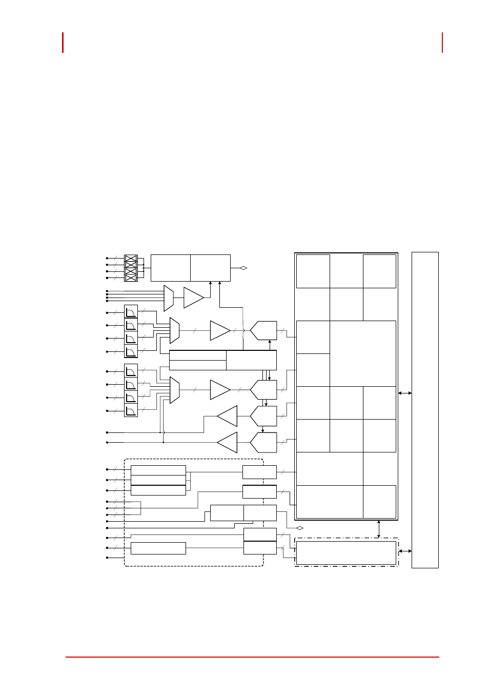
4 operation theory, 1 pci-9524 function diagram, Figure 4-1: pci-9524 function diagram – ADLINK PCI-9524 User Manual
Page 63: Pci-9524 function diagram, 4operation theory

Operation Theory
47
ADLINK Technology Inc.
Copyright 2008
4
Operation Theory
The operation theory of the functions of PCI-9524 are described in
this chapter. The functions include A/D conversion, D/A conver-
sion, pulse-commands, encoder inputs, and isolated digital I/O.
Operation theory helps users understand how to configure and
program PCI-9524.
4.1
PCI-9524 Function Diagram
Figure 4-1: PCI-9524 Function Diagram
M
U
X
SOA Protection
Voltage
Regulator
SPI BUS
Reference Voltage
Generator
SPI BUS
SPI BUS
Auto-zero
Controller
IIR Filter
Block
AD FIFO #0
AD FIFO #1
DMA
AI Timing Control
SPI BUS
Pulse Command Generator
Quadrature Decoder
Fast Polling
Port Control
M
U
X
Isolated DIO
M
U
X
Isolated
Barrier
Isolated
Power
ISO5VDD
DC-DC
Diff Pulse Driver #0
Isolated
Barrier
Isolated DO MOSFET
Diff Pulse Driver #1
Isolated
Barrier
Isolated
Barrier
Diff Pulse Driver #2
PCI 12V
PCI 5V
ADC
INA
PGA
DAC
OPAMP
ADC
DAC
OPAMP
OPAMP
Isolated Plane
Input Filter
2
2
2
2
2
2
2
2
2
2
2
2
2
2
2
2
2
2
2
2
2
2
2
2
2
2
2
4
4
4
4
6
6
8
8
8
8
2
2
2
Reference Bridge
Calibration Sources
VEX0
VEX1
VEX2
VEX3
VEX_SEN0
VEX_SEN1
VEX_SEN2
VEX_SEN3
AI0
AI1
AI2
AI3
AI4
AI5
AI6
AI7
AO0
AO1
PULSE0
PULSE1
PULSE2
ENC0
ENC1
ENC2
ISO5VDD
ISOPWR
IDI[7..0]
ID0[7..0]
ISOGND
P
C
I B
u
s C
o
n
tr
o
lle
r
Trigger
Interrupt
Controller
