11 floppy drive connector (fdd1), 12 sram. memory bank address select (xp3) – Acrosser AR-B1673 User Manual
Page 15
AR-B1673 User’s Guide
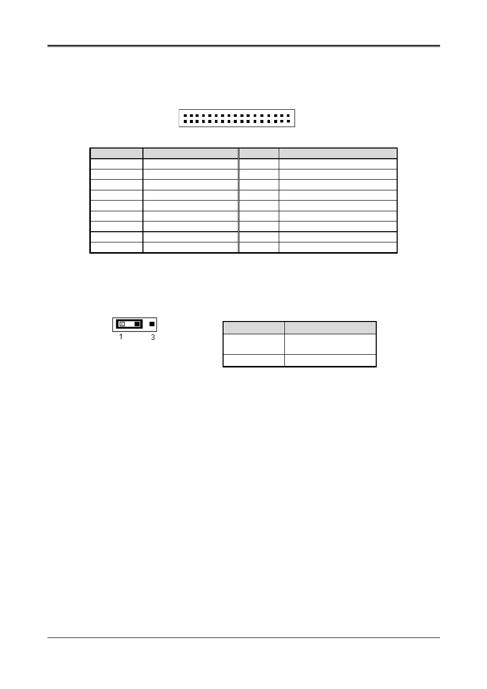
3.11 FLOPPY DRIVE CONNECTOR (FDD1)
The AR-B1673 provides a 34-pin header type connector for supporting up to two floppy disk drives.
To enable or disable the floppy disk controller, please use the BIOS Setup program.
33
34
1
2
PIN
Signal
PIN
Signal
1-33(odd) GROUND
18
DIRECTION
2
DRVEN 0
20
-STEP OUTPUT PULSE
4
NOT USED
22
-WRITE DATA
6
DRVEN 1
24
-WRITE GATE
8 -INDEX
26 -TRACK
0
10
-MOTOR ENABLE 0
28
-WRITE PROTECT
12
-DRIVE SELECT 1
30
-READ DATA
14
-DRIVE SELECT 0
32
-SIDE 1 SELECT
16
-MOTOR ENABLE 1
34
DISK CHANGE
3.12 SRAM. MEMORY BANK ADDRESS SELECT (XP3)
This section provides the information about how to use the SRAM. It divided into two parts: hardware setting and
software configuration.
Step 1: Use XP3 to select the correct SRAM memory address.
XP3
ADDRESS
1-2
D000
(Factory Preset)
2-3 D800
Step 2: Insert programmed SRAM into IC U18 setting as SRAM.
The hardware divides every 8KB of memory into a memory bank. User to assign a bank number,
Memory bank start from 00, last memory bank number depends on the size to the SRAM chip.
If on board the 512KB SRAM chip, the memory bank in the range of 00 to 63. The SRAM I/O Port =
200H
.
Example: Select the 10th bank of the U18. Using 512K*8, the I/O port =200H
Answer 1:(in assembly language)
MOV DX, 200H ; AR-B1673’s I/O port=200h
MOV AL, 10 ; Selection the 10th bank
OUT DX, AL ;
Answer 2: (in Basic language)
OUT &H200,&10 : AR-B1673’s I/O port=200h
Answer 3:(in Turbo C language)
Outportb(0x200,10)
15