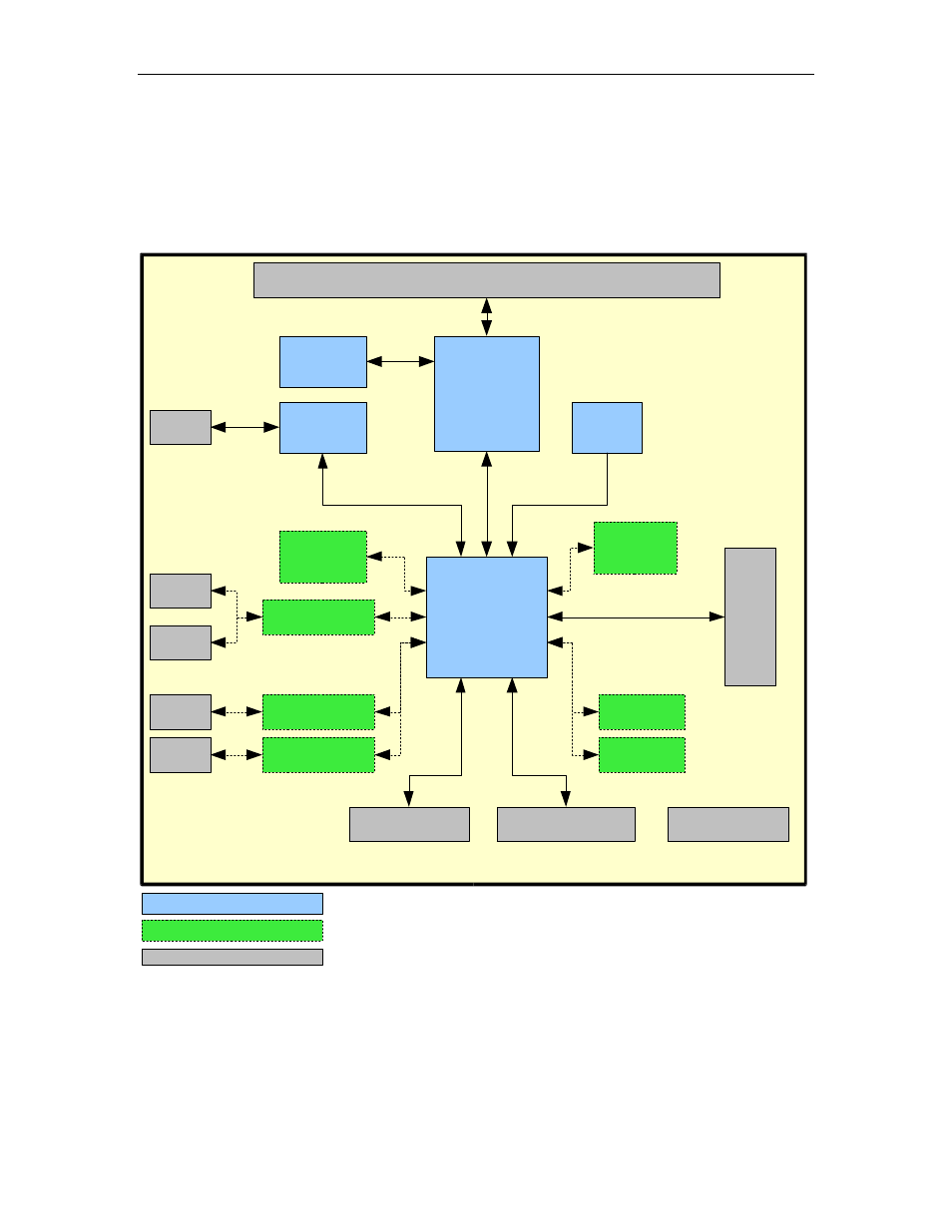
System overview, Figure 1: freeform/pci-104 block diagram – Connect Tech PCI-104 User Manual
Page 7

Connect Tech FreeForm/PCI-104 User Manual
Revision 0.02
7
System Overview
The following conceptual block diagram provides a high level overview of the FreeForm/PCI-104 and
illustrates the general interconnection between components and connectors.
For the actual orientation and description of components refer to Figure 2 and Table 1 respectively.
FPGA
[Xilinx Virtex-5]
PCI-104 Bus
2x40
Header
JTAG Connector
1x7 Header
64 I/O, 32 LVDS Pairs
Ext Power Connector
Dual Ethernet PHY
RS-485 Transceiver
PCI Bus Interface
[PLX 9056]s
SPI Flash
(FPGA
Config.)
Local Bus
1x6
Header
RJ-45
2x5
Header
Peripheral Circuitry
Core Circuitry
RS-485 Transceiver
2x5
Header
RJ-45
Connector
DDR2 RAM
SPI Flash
(Embedded
Code)
EEPROM
(Parameters)
DDR2 RAM
100 Mhz
Osc.
High Speed Serial
EEPROM
(Config
Registers)
Figure 1: FreeForm/PCI-104 Block Diagram
