Connector pinouts, Pci-104 header (p1), Jtag programming header (p2) – Connect Tech PCI-104 User Manual
Page 11: Spi flash programming header (p3), Table 4: jtag programming header pinout (p2), Table 5: spi flash programming header pinout (p3)

Connect Tech FreeForm/PCI-104 User Manual
Revision 0.02
11
Connector Pinouts
PCI-104 Header (P1)
Refer to
Note: P1 must be connected to a PCI-104 stack supplying both 3.3V and 5V.
JTAG Programming Header (P2)
Use P2 to configure the FPGA via JTAG. Refer to
Power pins are for voltage reference only; they do not provide power to the configuration
circuitry.
Note that the FPGA can always be programmed via JTAG, regardless of the
setting.
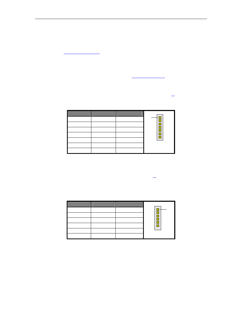
Table 4: JTAG Programming Header Pinout (P2)
Pin
Signal
Direction
1
TRST
Input
2
TMS
Input
3
TDI
Input
4
TDO
Output
5
TCK
Input
6
GND
Reference
7
3.3V
Reference
P
2
J
T
A
G
H
e
a
d
e
r
1
Top View
SPI Flash Programming Header (P3)
P3 may be used to directly program the SPI flash, providing that
is set correctly to the tri-state
FPGA position. The power pins are for voltage reference only. They do not provide power to the
configuration circuitry.
Table 5: SPI Flash Programming Header Pinout (P3)
Pin
Signal
Direction
1
SPI_CSN
Input
2
SPI_MOSI
Input
3
SPI_MISO
Output
4
SPI_CLK
Input
5
GND
Reference
6
3.3V
Reference
1
P
3
S
P
I
F
la
s
h
H
e
a
d
e
r
Top View
