Cp390 hotswap – Kontron CP390 User Manual
Page 30
CP390
Hotswap
ID 19976, Rev. 0200
Page 4 - 8
® PEP Modular Computers GmbH
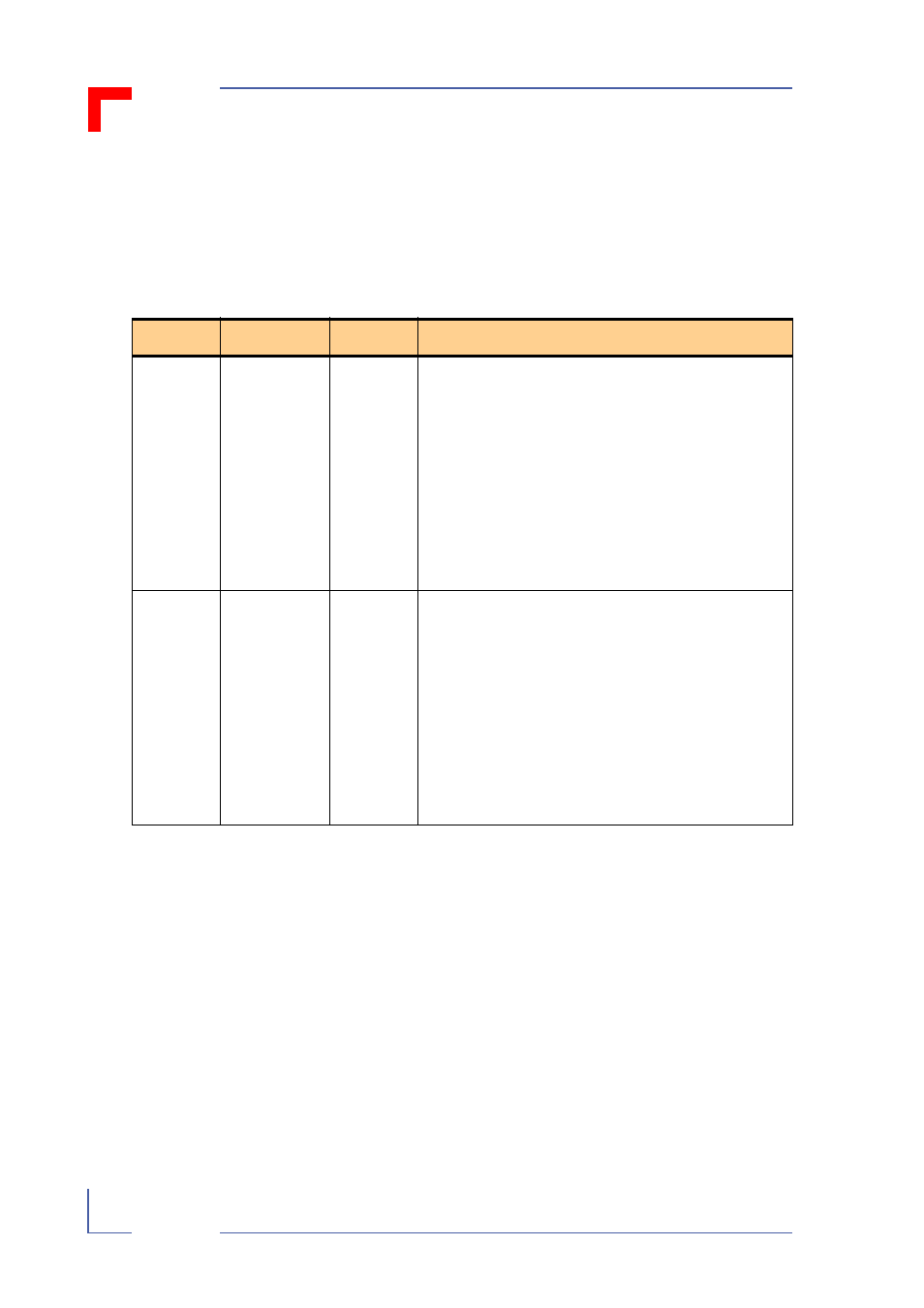
4.2.6.3 GPIO Output Data Register - Offset 65h
This section describes the GPIO output data register.
Dword address = 64h
Byte enable p_cbe_1<3:0> = xx0xb
Table 4-5: GPIO Output Data Register - Offset 65h
Dword Bit
Name
R/W
Description
11:8
GPIO output
enable write-
1-to-clear
R/W1TC
The gpio<3:0> pin output data
write-1-to-clear. Writing 1 to any of these bits drives
the corresponding bit low on the gpio<3:0> bus if it is
programmed as bi-directional. Data is driven on the
PCI clock cycle following completion of the
configuration write to this register. Bit positions cor-
responding to gpio pins that are programmed as input
only are not driven.
Writing 0 to these bits has no effect.
When read, reflects the last value written.
Reset value: 0.
15:12
GPIO output
enable write-
1-to-set
R/W1TS
The gpio<3:0> pin output data
write-1- to-set. Writing 1 to any of these bits drives
the corresponding bit high on the gpio<3:0> bus if it
is programmed as bi-directional. Data is driven on the
PCI clock cycle following completion of the
configuration write to this register. Bit positions cor-
responding to gpio pins that are programmed as input
only are not driven.
Writing 0 to these bits has no effect.
When read, reflects the last value written.
Reset value: 0.