Configuration, Cp390 configuration, 1 pinouts – Kontron CP390 User Manual
Page 21: 1 jn1 (con2) pin assignment
CP390
Configuration
ID 19976, Rev. 0200
Page 3 - 2
® PEP Modular Computers GmbH
3. Configuration
3.1 Pinouts
3.1.1
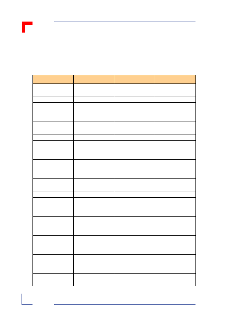
Jn1 (CON2) Pin Assignment
Table 3-1: Jn1, 32-bit PCI
Pin Number
Signal Name
Signal Name
Pin Number
1
TCK
-12V
2
3
Ground
INTA#
4
5
INTB#
INTC#
6
7
BUSMODE1#
+5V
8
9
INTD#
PCI-RSVD*
10
11
Ground
PCI-RSVD*
12
13
CLK
Ground
14
15
Ground
GNT#
16
17
REQ#
+5V
18
19
V(I/O)
AD[31]
20
21
AD[28]
AD[27]
22
23
AD[25]
Ground
24
25
Ground
C/BE[3]#
26
27
AD[22]
AD[21]
28
29
AD[19]
+5V
30
31
V(I/O)
AD[17]
32
33
FRAME#
Ground
34
35
Ground
IRDY#
36
37
DEVSEL#
+5V
38
39
Ground
LOCK#
40
41
SDONE#
SBO#
42
43
PAR
Ground
44
45
V(I/O)
AD[15]
46
47
AD[12]
AD[11]
48
49
AD[09]
+5V
50
51
Ground
C/BE[0]#
52
53
AD[06]
AD[05]
54
55
AD[04]
Ground
56
57
V(I/O)
AD[03]
58
59
AD[02]
AD[01]
60
61
AD[00]
+5V
62
63
Ground
REQ64#
64
See also other documents in the category Kontron Hardware:
- CP3003-SA uEFI BIOS (72 pages)
- CP3003-SA (36 pages)
- CP3002 (38 pages)
- CP3002-RC uEFI (64 pages)
- CP-RIO3-05 (42 pages)
- CP3002-RC (30 pages)
- CP342 (52 pages)
- CP930 (46 pages)
- CP932 (52 pages)
- CP346 (72 pages)
- CP384 (66 pages)
- CP383 (74 pages)
- CP382 (58 pages)
- CP381 (60 pages)
- CP372 (64 pages)
- CP371 (60 pages)
- CP-RIO3-04S (38 pages)
- CPS3410 (9 pages)
- CPS3402 (9 pages)
- CPS3105 (9 pages)
- CPS3101 (9 pages)
- CPS3003-SA (19 pages)
- PB-SIO4 (34 pages)
- PB-SIO4A (34 pages)
- PB-DOUT8 (34 pages)
- VMOD-2 (82 pages)
- VSBC-32 (110 pages)
- VM42 (62 pages)
- Bootstrap Loader (24 pages)
- VMP1 with Netbootloader (120 pages)
- VMP1 (106 pages)
- NetBootLoader (86 pages)
- VMP2 (142 pages)
- VMP3 (154 pages)
- CP-RIO6-923 (32 pages)
- CP-RIO6-923-F (32 pages)
- CP-RIO6-001 (28 pages)
- CP-RIO6-001-HD-VGA (46 pages)
- CP-RIO6-M (20 pages)
- CP-RIO6-B (28 pages)
- CP6925 (42 pages)
- CP6002 uEFI BIOS (76 pages)
- CP6002 IPMI (40 pages)
- CP6002 (42 pages)