Cool-oring, Pi2002 product description – Vicor PI2002-EVAL1 Active ORing With Load Disconnect Evaluation Board User Manual
Page 2

Picor Corporation • www.picorpower.com
PI2002-EVAL1 User Guide Rev 1.0 Page 2 of 11
The Cool-ORing™ PI2002 with two external back-to-back
configured industry standard N-channel MOSFETs is a
complete Active ORing solution that also provides a Load
Disconnect feature designed for use in redundant power
system architectures. The PI2002 controls back-to-back
MOSFETs providing true bi-directional switch capabilities to
protect against both power source and load fault conditions.
The gate drive output turns the MOSFETs on in normal steady
state operation, while achieving high-speed turn-off under
a variety of potential system-level fault conditions, per
conventional Active ORing solutions with auto-reset once
the fault clears. The PI2002 has the added benefit of being
able to protect against output load fault conditions that
may induce excessive forward current and device over-
temperature by removing gate drive from the MOSFETs
with an auto-retry programmable off-time. The back-to-back
MOSFETs drain-to-drain voltage is monitored to detect
normal forward, excessive forward, light load and reverse
current flow. The PI2002 provides an active low fault flag
output to the system during excessive forward current,
reverse current, light load, under-voltage, over-voltage and
over-temperature. A temperature sensing function turns
off the MOSFETs and indicates a fault if the junction
temperature exceeds 145°C.
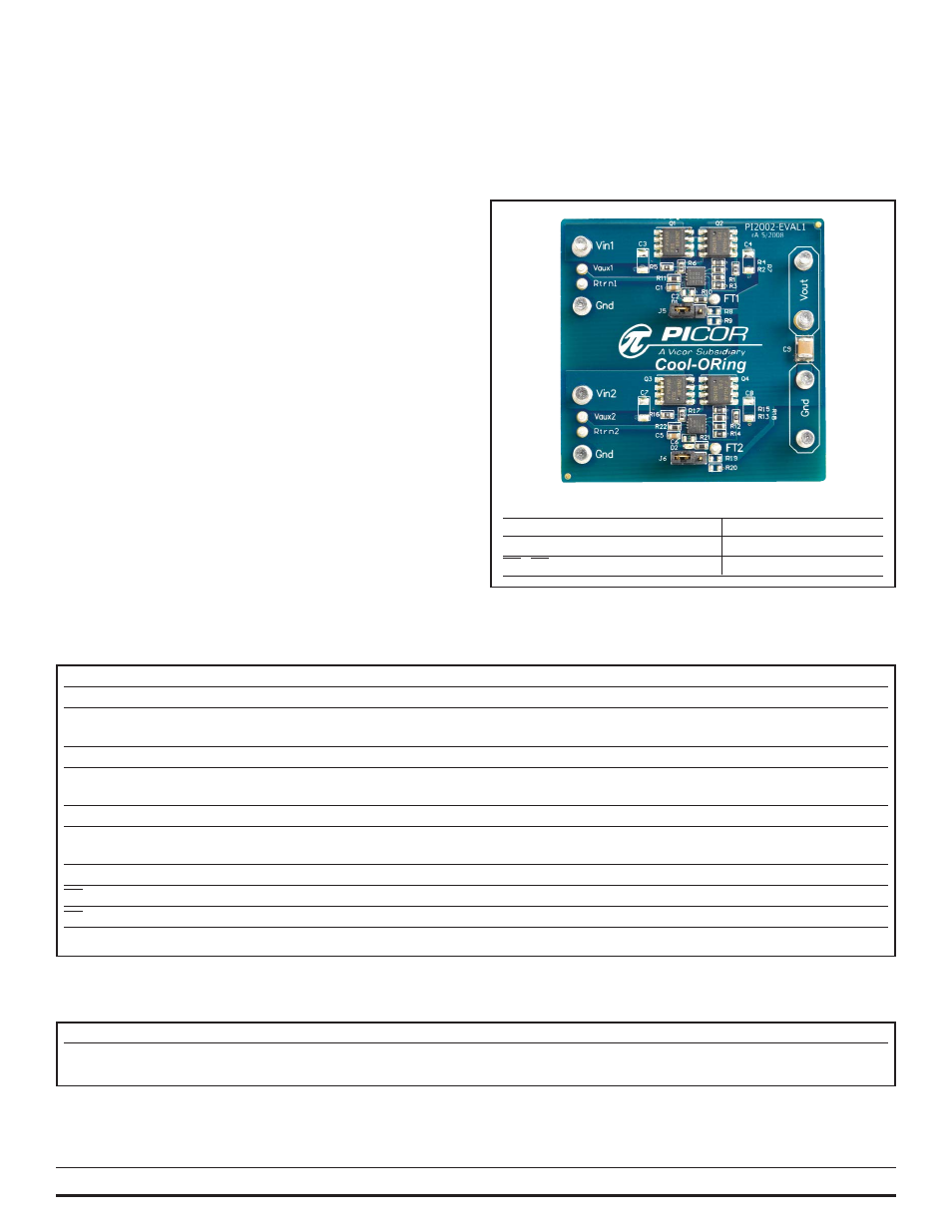
Figure 1 shows a photo of the PI2002-EVAL1 evaluation
board, with two PI2002 controllers and four N-channel
MOSFETs used to form the two Active ORing channels that
also feature a Load Disconnect function. The board is built
with two identical Active ORing circuits with options and
features that enable the user to fully explore the capabilities
of the PI2002 universal Active ORing with Load Disconnect
controller.
Figure 1 – PI2002-EVAL1 Evaluation Board (1.8" x 1.8")
Terminals Rating
Vin1, Vin2
8 V / 20 A
Vaux1, Vaux2, (R11 = R19 = 10
Ω
)
-0.3 V to 17.3 V / 40 mA
FT1, FT2
-0.3 V to 17.3 V / 10 mA
Terminal
Description
Vin1
Power Source Input #1 or bus input designed to accommodate up to 20 A continuous current.
Vaux1
Auxiliary Input Voltage #1 to supply PI2002 VC power. Vaux1 should be equal to Vin1 plus 5 V or higher.
See details in Auxiliary Power Supply (Vaux) section of the PI2002 data sheet.
Rtn1
Vaux1 Return Connection: Connected to Ground plane
Gnd
Vin & Vout Return Connection: Three Gnd connections are available and are connected to a common point, the Ground
plane. Input supplies Vin1 & Vin2 and the output load at Vout should all be connected to their respective local Gnd connection.
Vin2
Power Source Input #2 or bus input designed to accommodate up to 20 A continuous current.
Vaux2
Auxiliary Input Voltage #2 to supply PI2002 VC power. Vaux2 should be equal to Vin2 plus 5 V or higher.
See details in Auxiliary Power Supply (Vaux) section of the PI2002 data sheet.
Rtn2
Vaux2 Return Connection: Connected to Ground plane
FT1
PI2002 (U1) Fault Pin: Monitors U1 fault conditions
FT2
PI2002 (U2) Fault Pin: Monitors U2 fault conditions
Vout
Output: Q2 and Q4 MOSFET Drain pins connection, connect to the load high side.
Table 1 – PI2002-EVAL1 Evaluation Board terminals description
Cool-ORing
TM
PI2002 Product Description
Jumper
Description
J5, J6
SCD Jumpers: Connect jumper across the two pins to the input side (GND) for maximum Gate charge current or across
the two pins on the output side to connect to the resistive voltage divider to the output.
Table 2 – PI2002-EVAL1 Evaluation Board jumpers description
