Edb9315a circuit description, Figure 3. block diagram – Cirrus Logic EDB9315A User Manual
Page 10

EDB9315A
Technical Reference Manual
10
©
Copyright 2006 Cirrus Logic, Inc.
DS638DB3
4. EDB9315A Circuit Description
This chapter makes reference to the schematics in Appendix A and discusses the main circuit
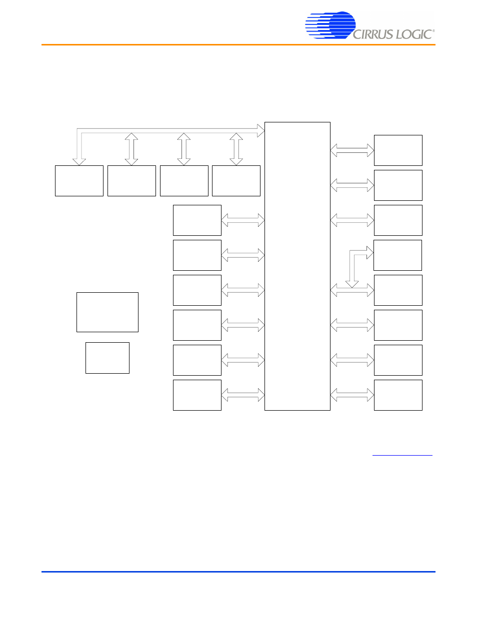
functionality of each schematic page. A detailed block diagram of the EDB9315A Engineering
Development Board is shown below.
Figure 3. Block Diagram
Detailed information regarding the EP9315 processor and interfaces can be found
.
The details of this device will not be discussed in this document. Refer to the EP9315 datasheet, User's
Guide, and other information on the web site for more information.
Audio In
Audio Out
EP9315
IDE
40 pin
VGA
DB15
LCD
40 pin
Dual USB 2. 0
Host
( Full Speed)
Flash
16 MByte
16-bit
Peripheral
Expansion
120 pin
JTAG
20 pin
Touchscreen
10 pin
UART1
DB9 w/ control
UART2
UART3
10 pin
Ethernent
RJ45
Serial
EEPROM
POWER
Vin = +12V
Vout=1.8 , 3.3 , 5.0
USB 2. 0
Device
( High Speed)
SDRAM
64 MByte
32-bit
Memory
Expansion
120 pin
CIR
Reset and
voltage
monitoring
RTC
battery backed
