An74, Maximum sclk rate, Development tool description – Cirrus Logic AN74 User Manual
Page 4
AN74
4
AN74Rev2
An alternative method can be used to acquire a con-
version. By clearing the Port Flag bit, the serial
port’s function isn’t modified. The Done Flag bit
(bit three in the configuration register) can be
polled as it indicates when a conversion is compete
and ready to acquire. The conversion is acquired by
reading the conversion data register.
MAXIMUM SCLK RATE
A machine cycle in the 80C51 consists 12 oscillator
periods or 1
µ
s if the microcontroller’s oscillator
frequency is 12 MHz. Since the CS5525/6/9’s max-
imum SCLK rate is 2MHz, additional no operation
(NOP) delays may be necessary to reduce the trans-
fer rate if the microcontroller system requires high-
er rate oscillators.
DEVELOPMENT TOOL DESCRIPTION
The code in the application note was developed us-
ing a software development package from Franklin
Software, Inc. The code consists of intermixed C
and assembler algorithms which are subsets of the
algorithms used by the CDB5525/6/9, a customer
evaluation board from Crystal Semiconductor.
Moreover, Franklin’s A51 Assembler, C51 Com-
piler, and L51 Linker development software were
used to generate the run-time software for the mi-
crocontroller on the CDB5526.
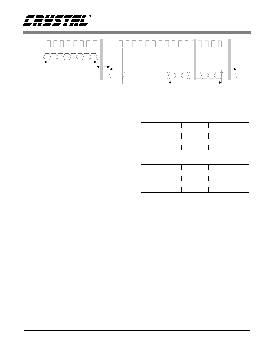
Command Time
8 SCLKs
8 SCLKs Clear SDO Flag
Data SDO Continuous Conversion Read (PF bit = 1)
SDO
SCLK
SDI
t *
d
Data Time
24 SCLKs
MSB
LSB
* td = XIN/OWR clock cycles for each conversion except the
first conversion which will take XIN/OWR + 7 clock cycles
XIN/OWR
Clock Cycles
Figure 5. Conversion/Acquisition Cycle with PF Bit Asserted
MSB
High-Byte
Mid-Byte
Low-Byte
A) 20-Bit Conversion Data Word
MSB
High-Byte
Mid-Byte
Low-Byte
B) 16-Bit Conversion Data Word
0- always zero, 1
-
always one,
OD - Oscillation Detect, OF - Overflow
Figure 6. Bit Representation/Storage in PIC16F84
D19
D18
D17
D16
D15
D14
D13
D12
D11
D10
D9
D8
D7
D6
D5
D4
D3
D2
D1
D0
0
0
OD
OF
D15
D14
D13
D12
D11
D10
D9
D8
D7
D6
D5
D4
D3
D2
D1
D0
1
1
1
1
0
0
OD
OF