Cirrus Logic AN74 User Manual
Cirrus Logic Hardware
1
Copyright
Cirrus Logic, Inc. 1997
(All Rights Reserved)
Cirrus Logic, Inc.
Crystal Semiconductor Products Division
P.O. Box 17847, Austin, Texas 78760
(512) 445 7222 FAX: (512) 445 7581
http://www.crystal.com
AN74
Application Note
Interfacing the CS5525/6/9 to the 80C51
By Keith Coffey
INTRODUCTION
This application note details the interface of Crys-
tal Semiconductor’s CS5525/6/9 Analog-to-Digi-
tal Converter (ADC) to an 80C51 microcontroller.
This note takes the reader through a simple exam-
ple describing how to communicate with the ADC.
All algorithms discussed are included in the Ap-
pendix at the end of this note.
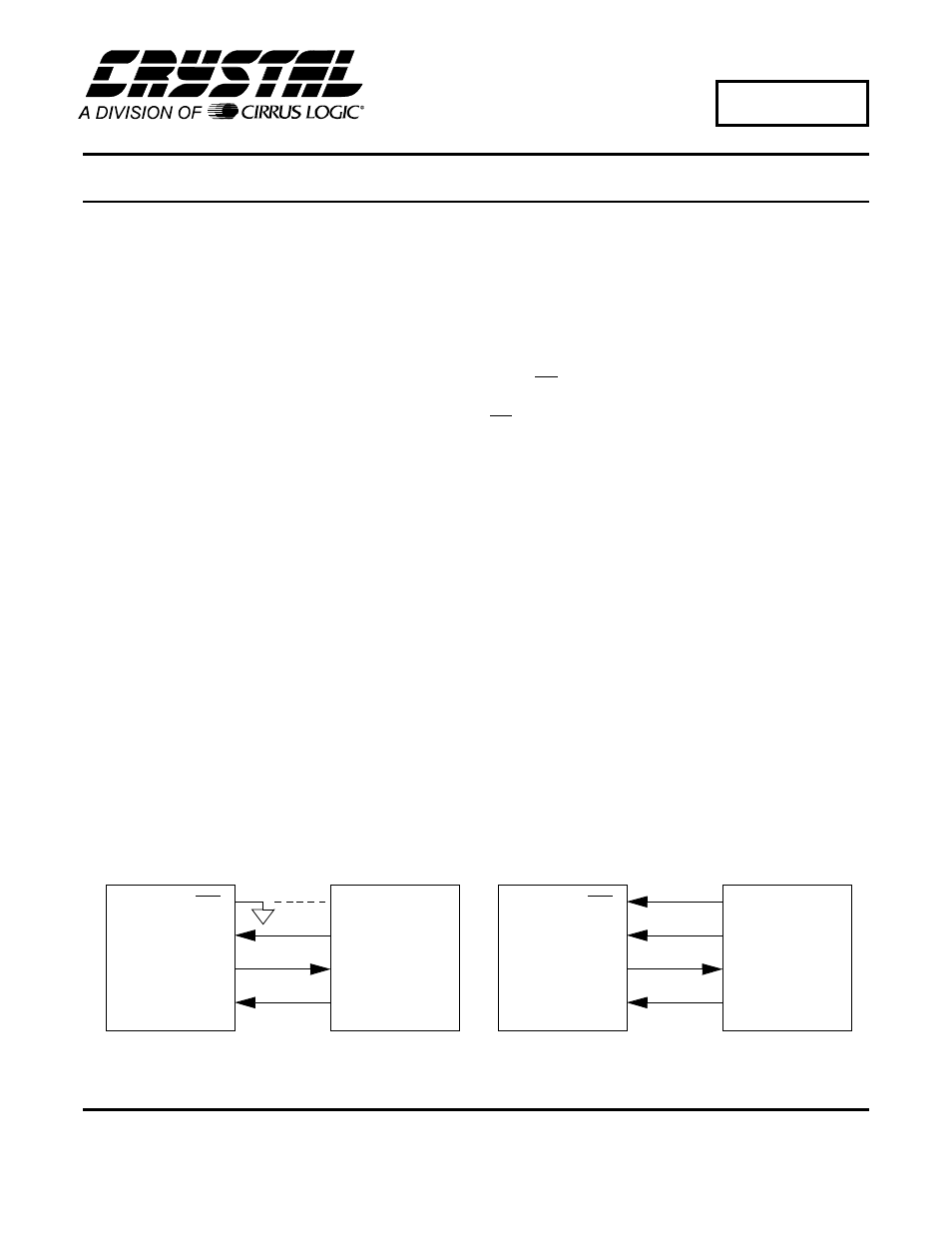
ADC DIGITAL INTERFACE
The CS5525/6/9 interfaces to the 80C51 through
either a three-wire or a four-wire interface. Figure
1 depicts the interface between the two devices.
Though this software was written to interface to
Port 1 (P1) on the 80C51 with a four-wire interface,
the algorithms can be easily modified to work with
the three-wire format.
The ADC’s serial port consists of four control
lines: CS, SCLK, SDI, and SDO.
CS, Chip Select, is the control line which enables
access to the serial port.
SCLK, Serial Clock, is the bit-clock which controls
the shifting of data to or from the ADC’s serial
port.
SDI, Serial Data In, is the data signal used to trans-
fer data from the 80C51 to the ADC.
SDO, Serial Data Out, is the data signal used to
transfer output data from the ADC to the 80C51.
SOFTWARE DESCRIPTION
This note presents algorithms to initialize the
80C51 and the CS5525/6/9, perform self-offset cal-
ibration, modify the CS5525/6/9’s gain register,
and acquire a conversion. Figure 2 depicts a block
CS5525/6/9
80C51
P1.0
P1.1
P1.2
P1.3
CS
SDI
SDO
SCLK
Figure 1. 3-Wire and 4-Wire Interfaces
CS5525/6/9
80C51
P1.0 (logic 0)
P1.1
P1.2
P1.3
CS
SDI
SDO
SCLK
NOV ‘97
AN74Rev2