Cirrus Logic CDB53L21 User Manual
Cdb53l21, Evaluation board for cs53l21, Features
Copyright
© Cirrus Logic, Inc. 2006
(All Rights Reserved)
Evaluation Board for CS53L21
Features
Selectable Analog Inputs
–
Stereo Line-Level RCA Jacks
–
Stereo Microphone 1/8” Jacks
Stereo Microphone Input Jacks
8- to 96-kHz S/PDIF Output
–
CS8406 Digital Audio Transmitter
I/O Stake Headers
–
External Control Port Accessibility
–
External DSP Serial Audio I/O Accessibility
Independent, Regulated Supplies
1.8 V to 3.3 V Logic Interface
Hardware Control
–
4 Pre-Defined Switch Settings
FlexGUI S/W Control - Windows
®
Compatible
–
Pre-Defined & User-Configurable Scripts
Layout and Grounding Recommendations
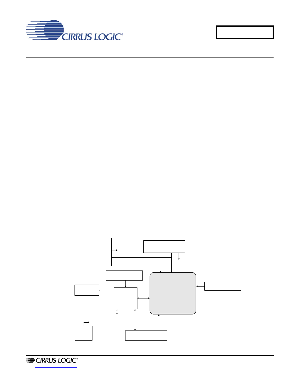
Description
The CDB53L21 evaluation board is an excellent means
for evaluating the CS53L21 ADC. Evaluation requires
an analog audio source, an analog/digital analyzer and
power supplies. Optionally, a Windows
PC-compatible
computer may be used to evaluate the CS53L21 in Soft-
ware Mode.
System timing can be provided by the CS53L21 with
supplied master clock, or by using an I/O stake header
with a DSP connected.
RCA phono jacks are provided for the CS53L21 analog
inputs. 1/8” jacks are also available for microphone in-
puts. A digital data output is available from the CS8406
via RCA phono or optical connectors.
The Windows software provides a GUI to make config-
uration of the CDB53L21 easy. The software
communicates through the PC’s serial port or USB port
to configure the control port registers so that all features
of the CS53L21 can be evaluated. The evaluation board
may also be configured to accept external timing and
data signals for operation in a user application during
system development.
ORDERING INFORMATION
CDB53L21
Evaluation Board
Analog Input
(Line or MIC)
Software Mode
Control Port
CS53L21
S/PDIF Output
(CS8406)
Clocks/Data Header
I²C/SPI Header
FPGA
Oscillator
(socket)
Reset
MCLK
Reset
Reset
MCLK
Reset
Hardware Mode
Switches
MARCH '06
DS700DB1
CDB53L21
Document Outline
- 1. System Overview
- 2. Software Mode Control
- 3. Hardware Mode Control
- 4. Performance Plots
- Figure 10. 0 dB FFT, Single-Speed Mode
- Figure 11. 0 dB FFT, Double-Speed Mode
- Figure 12. -60 dB FFT, Single-Speed Mode
- Figure 13. -60 dB FFT, Double-Speed Mode
- Figure 14. No Input FFT, Single-Speed Mode
- Figure 15. No Input FFT, Double-Speed Mode
- Figure 16. THD+N vs. Frequency, Single-Speed Mode
- Figure 17. THD+N vs. Frequency, Double-Speed Mode
- Figure 18. THD+N vs. Amplitude, Single-Speed Mode
- Figure 19. THD+N vs. Amplitude, Double-Speed Mode
- Figure 20. Fade-to-Noise Linearity, Single-Speed Mode
- Figure 21. Fade-to-Noise Linearity, Double-Speed Mode
- Figure 22. Frequency Response, Single-Speed Mode
- Figure 23. Frequency Response, Double-Speed Mode
- Figure 24. Channel Crosstalk, Single-Speed Mode
- Figure 25. Channel Crosstalk, Double-Speed Mode
- 5. System Connections and Jumpers
- 6. Block Diagram
- 7. Schematics
- Figure 27. CS53L21 (Part of Schematic Sheet 1)
- Figure 28. Analog I/O (Part of Schematic Sheet 1)
- Figure 29. S/PDIF I/O (Schematic Sheet 2)
- Figure 30. FPGA (Schematic Sheet 3)
- Figure 31. Level Shifters & I/O Stake Header (Schematic Sheet 4)
- Figure 32. Control Port I/O (Schematic Sheet 5)
- Figure 33. Power (Schematic Sheet 6)lm
- 8. Board Layout
- 9. Revision History