Typical connection diagrams, Figure 1. cs5381 typical connection diagram, Figure 2. ak5394a typical connection diagram – Cirrus Logic AN234 User Manual
Page 2: An234
AN234
2
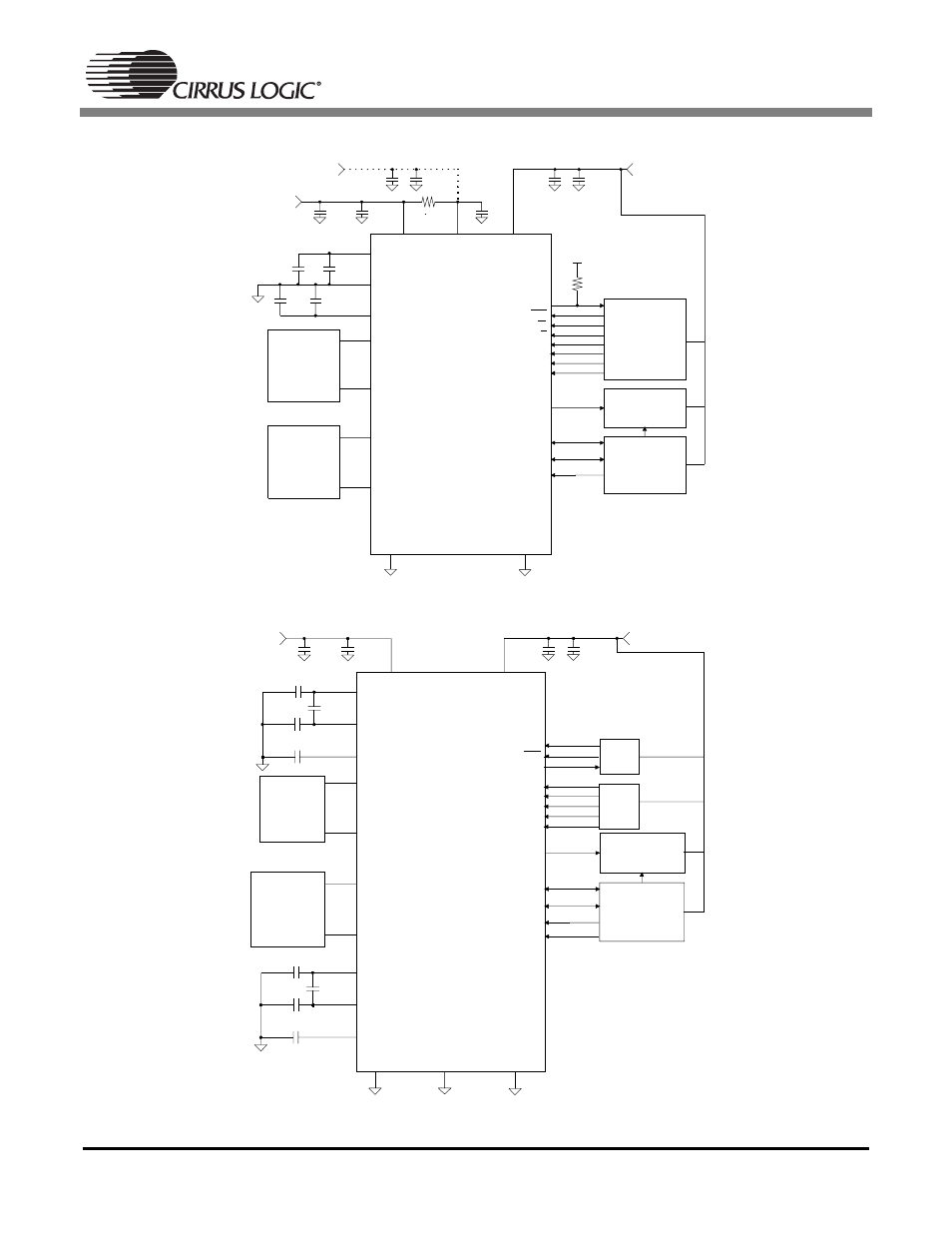
2. Typical Connection Diagrams
Figure 1. CS5381 Typical Connection Diagram
Figure 2. AK5394A Typical Connection Diagram
FILT+
AINL+
AINL-
V
D
0.1
µ
F
A/D CONVERTER
SCLK
CS5381
M /S
MCLK
AINR+
AINR-
VQ
200
µ
F
+
RST
VA
V
L
+5V
1
µ
F
+5V to 2.5V
5.1
Ω
1
µ
F
+
+
+
SDOUT
GND
I
2
S/LJ
LRCK
GND
Power Down
and Mode
Settings
Audio Data
Processor
Timing Logic
and Clock
0.1
µ
F
0.1
µ
F
0.1
µ
F
0.1
µ
F
HPF
M0
M1
REFGND
MDIV
+5 V to 3.3 V
1
µ
F
0.1
µ
F
1
µ
F
+
Analog
Input
Buffer
(Section 8)
Analog
Input
Buffer
(Section 8)
OVFL
10 k
VL
*
*
Resistor may only
be used if VD is
derived from VA. If
used, do not drive
any other logic
from VD.
VREFL+
AINL+
AINL-
V
A/D CONVERTER
AK5394A
AINR+
AINR-
VCOML
RST
VA
D
+5V
10
µ
F
+5V to 3.3V
10
µ
F
+
+
SDATA
CAL
Reset and
Calibration
Control
Audio Data
Processor
Timing Logic
and Clock
SMODE2
SMODE1
VREFL-
DFS0
Analog
Input
Buffer
(Section 8)
Analog
Input
Buffer
(Section 8)
ZCAL
0.1
AGND
DGND
BGND
µ
F
0.1
µ
F
VREFR+
VREFR-
HPFE
Mode
Control
LRCK
FSYNC
SCLK
MCLK
0.22
µ
F
+
+
C
C
0.22
µ
F
0.22
µ
F
+
+
C
C
0.22
µ
F
VCOMR
DFS1
*
*
*
*
* See Section 9