Cirrus Logic CS4391 User Manual
Preliminary product information, Features, Description
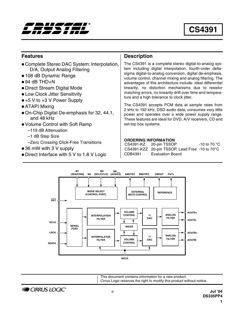
Table of contents
Document Outline
- 1. Characteristics/Specifications
- 2. Typical Connection DiagramS
- 3. Register qUICK rEFERENCE
- 4. Register Description
- 5. PIN DESCRIPTION - PCM Data mode
- Reset - RST
- Interface Power - VL
- Serial Audio Data - SDATA
- Serial Clock - SCLK
- Left / Right Clock - LRCK
- Master Clock - MCLK
- Mode Select - M3, M2, M1 and M0 (Stand-alone Mode)
- Mode Select - M3 (Control Port Mode)
- Serial Control Interface Clock - SCL/CCLK (Control Port Mode)
- Serial Control Data I/O - SDA/CDIN (Control Port Mode)
- Address Bit / Chip Select - AD0 / CS (Control Port Mode)
- Positive Voltage Reference - FILT+
- Common Mode Voltage - CMOUT
- Channel A and Channel B Mute Control - AMUTEC and BMUTEC
- Differential Analog Output - AOUTB+, AOUTB- and AOUTA+, AOUTA-
- Analog Ground - AGND
- Analog Power - VA
- 6. PIN DESCRIPTION - DSD mode
- DSD Audio Data - DSD_A and DSD_B
- DSD Mode - DSD_Mode
- Master Clock - MCLK
- DSD Serial Clock - DSD_SCLK
- Table 1. Digital Interface Formats - PCM Modes
- Table 2. Digital Interface Formats - DSD Mode
- Table 3. De-Emphasis Mode Selection
- Table 4. Functional Mode Selection
- Table 5. Soft Cross or Zero Cross Mode Selection
- Table 6. ATAPI Decode
- Table 7. Digital Volume Control
- Table 8. Single Speed (4 to 50 kHz sample rates) Common Clock Frequencies
- Table 9. Double Speed (50 to 100 kHz sample rates) Common Clock Frequencies
- Table 10. Quad Speed (100 to 200 kHz sample rates) Common Clock Frequencies
- Table 11. Single Speed (4 to 50 kHz) Digital Interface Format, Stand-Alone Mode Options
- Table 12. Single Speed Only (4 to 50 kHz) De-Emphasis, Stand-Alone Mode Options
- Table 13. Double Speed (50 to 100 kHz) Digital Interface Format, Stand-Alone Mode Options
- Table 14. Quad Speed (100 to 200 kHz) Digital Interface Format, Stand-Alone Mode Options
- Table 15. Direct Stream Digital (DSD), Stand-Alone Mode Options
- Figure 7. Format 0, Left Justified up to 24-Bit Data
- Figure 8. Format 1, I2S up to 24-Bit Data
- Figure 9. Format 2, Right Justified 16-Bit Data
- Figure 10. Format 3, Right Justified 24-Bit Data
- Figure 11. Format 4, Right Justified 20-Bit Data. (Available in Control Port Mode only)
- Figure 12. Format 5, Right Justified 18-Bit Data. (Available in Control Port Mode only)
- Figure 13. De-Emphasis Curve
- Figure 14. ATAPI Block Diagram
- 7. Applications
- 8. Control Port Interface
- 8.1 SPI Mode
- 8.2 I2C Mode
- Table 16. Memory Address Pointer (MAP)
- Figure 16. Control Port Timing, SPI mode
- Figure 17. Control Port Timing, I2C Mode
- Figure 18. Single-Speed Frequency Response
- Figure 19. Single-Speed Transition Band
- Figure 20. Single-Speed Transition Band
- Figure 21. Single-Speed Stopband Rejection
- Figure 22. Double-Speed Frequency Response
- Figure 23. Double-Speed Transition Band
- Figure 24. Double-Speed Transition Band
- Figure 25. Double-Speed Stopband Rejection
- 9. PARAMETER DEFINITIONS
- 10. REFERENCES
- 11. PACKAGE DIMENSIONS