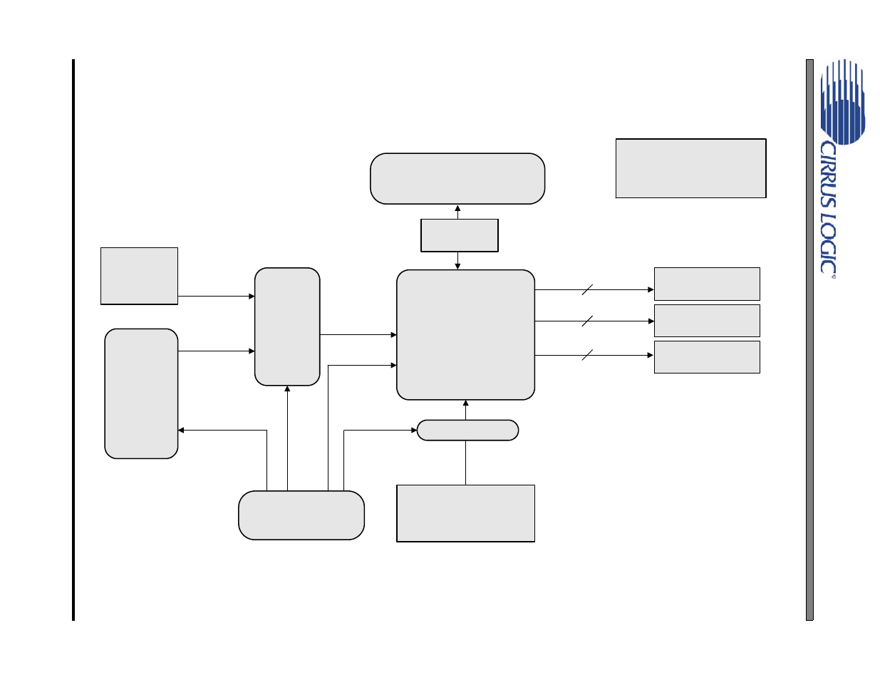
Cdb4365 schematics, Figure 43. system block diagram and signal flow, Figure 43.system block diagram and signal flow – Cirrus Logic CDB4365 User Manual
Page 17: Cs4365, Cs8416 s/pdif input serial control port pcm mux, 2dsd clk_enable, Hardware control switches
DS67
0DB3
17
CDB4365
9. CDB4365 SCHEMATICS
CS4365
CS8416
S/PDIF
Input
Serial Control Port
PCM mux
PCM Clocks/Data
PCM Clocks/Data
I
2
C/SPI Header
Power
D
S
D Clo
cks
/
Da
t
a
DSD HEADER
2
2
DSD clk_enable
PCM Clocks/Data
D
S
D
i
nput
enabl
e
M
0
- M
4
sw
it
c
h
e
s
(
fo
r
s
tand
-
alone
mode
)
PC
M s
ourc
e
se
le
c
t
C
S
841
6
c
lo
ck se
tt
in
g
Hardware Control
Switches
PCM HEADER
2
A1, B1
A2, B2
A3, B3
Differential to Single-Ended
Analog Outputs
Figure 43. System Block Diagram and SIgnal Flow
See also other documents in the category Cirrus Logic Hardware:
- CobraNet (147 pages)
- CS4961xx (54 pages)
- CS150x (8 pages)
- CS1501 (16 pages)
- CS1601 (2 pages)
- CS1601 (16 pages)
- CS1610 (16 pages)
- CRD1610-8W (24 pages)
- CRD1611-8W (25 pages)
- CDB1610-8W (21 pages)
- CS1610A (18 pages)
- CDB1611-8W (21 pages)
- CDB1610A-8W (21 pages)
- CDB1611A-8W (21 pages)
- CRD1610A-8W (24 pages)
- CRD1611A-8W (25 pages)
- CS1615 (16 pages)
- AN403 (15 pages)
- AN401 (14 pages)
- AN400 (15 pages)
- AN375 (27 pages)
- AN376 (9 pages)
- CRD1615-8W (22 pages)
- CRD1616-8W (23 pages)
- AN402 (14 pages)
- AN404 (15 pages)
- CRD1615A-8W (21 pages)
- CS1615A (16 pages)
- CS1630 (56 pages)
- AN374 (35 pages)
- AN368 (80 pages)
- CRD1630-10W (24 pages)
- CRD1631-10W (25 pages)
- CS1680 (16 pages)
- AN405 (13 pages)
- AN379 (31 pages)
- CRD1680-7W (31 pages)
- AN335 (10 pages)
- AN334 (6 pages)
- AN312 (14 pages)
- AN Integrating CobraNet into Audio Products (16 pages)
- CobraNet Audio Routing Primer (9 pages)
- Bundle Assignments in CobraNet Systems (3 pages)
- CS2300-01 (3 pages)
- CS2000-CP (38 pages)