Figure 18. dsd phase modulation mode diagram, 9 grounding and power supply arrangements, 1 capacitor placement – Cirrus Logic CS4365 User Manual
Page 27: Figure 18.dsd phase modulation mode diagram, Figure 18, Cs4365
DS670F2
27
CS4365
4.9
Grounding and Power Supply Arrangements
As with any high-resolution converter, the CS4365 requires careful attention to power supply and grounding
arrangements if its potential performance is to be realized. The Typical Connection Diagram shows the rec-
ommended power arrangements, with VA, VD, VLC, and VLS connected to clean supplies. If the ground
planes are split between digital ground and analog ground, the GND pins of the CS4365 should be connect-
ed to the analog ground plane.
All signals, especially clocks, should be kept away from the FILT+ and VQ pins in order to avoid unwanted
coupling into the DAC.
4.9.1
Capacitor Placement
Decoupling capacitors should be placed as close to the DAC as possible, with the low value ceramic ca-
pacitor being the closest. To further minimize impedance, these capacitors should be located on the same
layer as the DAC. If desired, all supply pins with similar voltage ratings may be connected to the same
supply, but a decoupling capacitor should still be placed on each supply pin.
Notes: All decoupling capacitors should be referenced to ground.
The CDB4365 evaluation board demonstrates the optimum layout and power supply arrangements.
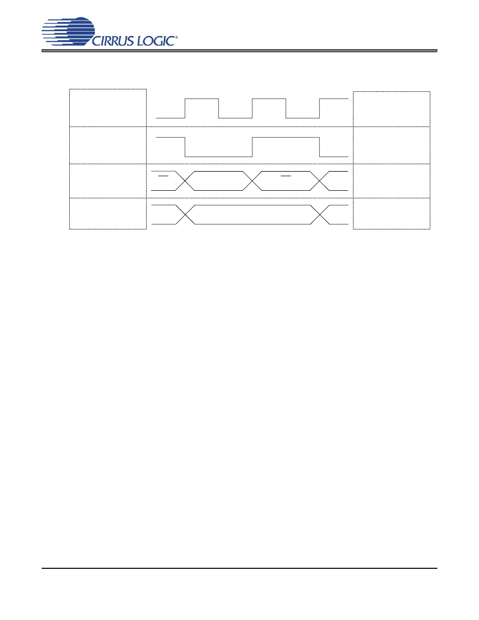
BCKA
(128Fs)
BCKD
(64Fs)
DSD_SCLK
DSDAx,
DSDBx
D1
D1
D1
D0
D2
D2
D0
DSD_SCLK
DSDAx,
DSDBx
BCKA
(64Fs)
DSD_SCLK
DSD Phase
Modulation Mode
DSD Normal Mode
Not Used
Not Used
Not Used
Figure 18. DSD Phase Modulation Mode Diagram