Cirrus Logic CS4365 User Manual
Cs4365, Channel d/a converter, Features
Copyright
© Cirrus Logic, Inc. 2008
(All Rights Reserved)
114 dB, 192 kHz
6
-Channel D/A Converter
Features
Advanced Multi-bit Delta Sigma Architecture
24-bit Conversion
Automatic Detection of Sample Rates up to
192 kHz
114 dB Dynamic Range
-100 dB THD+N
Direct Stream Digital Mode
–
Non-Decimating Volume Control
–
On-Chip 50 kHz Filter
–
Matched PCM and DSD Analog Output
Levels
Selectable Digital Filters
Volume Control with 1/2-dB Step Size and Soft
Ramp
Low Clock-Jitter Sensitivity
+5 V Analog Supply, +2.5 V Digital Supply
Separate 1.8 to 5 V Logic Supplies for the
Control and Serial Ports
Description
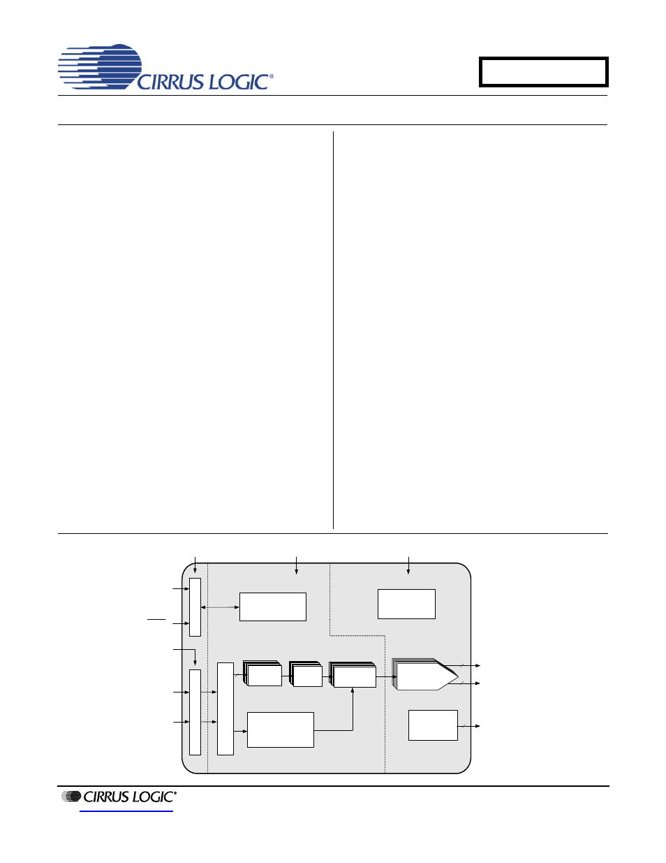
The CS4365 is a complete 6-channel digital-to-analog
system. This D/A system includes digital de-emphasis,
half-dB step size volume control, ATAPI channel mix-
ing, selectable fast and slow digital interpolation filters
followed by an oversampled, multi-bit delta sigma mod-
ulator which includes mismatch-shaping technology
that eliminates distortion due to capacitor mismatch.
Following this stage is a multi-element switched capac-
itor stage and low-pass filter with differential analog
outputs.
The CS4365 also has a proprietary DSD processor
which allows for volume control and 50 kHz on-chip fil-
tering without an intermediate decimation stage. It also
offers an optional path for direct DSD conversion by di-
rectly using the multi-element switched capacitor array.
The CS4365 is available in a 48-pin LQFP package in
both Commercial (-40°C to +85°C) and Automotive
(-40°C to +105°C) grades. The CDB4365 Customer
Demonstration board is also available for device evalu-
ation and implementation suggestions. Please see
“Ordering Information” on page 51
for complete details.
The CS4365 accepts PCM data at sample rates from
4 kHz to 216 kHz, DSD audio data, and delivers excel-
lent sound quality. These features are ideal for multi-
channel audio systems, including SACD players, A/V
receivers, digital TV’s, mixing consoles, effects proces-
sors, sound cards, and automotive audio systems.
Control Port Supply = 1.8 V to 5 V
Register/Hardware
Configuration
Internal Voltage
Reference
Reset
Ser
ia
l Interfac
e
Lev
e
l T
ran
slat
or
Level
Tr
an
s
lator
Digital Supply = 2.5 V
Hardware Mode or
I
2
C/SPI Software Mode
Control Data
Analog Supply = 5 V
Six Channels of
Differential
Outputs
6
6
PCM Serial
Audio Input
Volume
Controls
Digital
Filters
Switch-Cap
DAC and
Analog Filters
Multi-bit
ΔΣ
Modulators
DSD Audio
Input
DSD Processor
-Volume control
-50 kHz filter
External Mute
Control
Mute Signals
6
6
Serial Audio Port
Supply = 1.8 V to 5 V
FEB '08
DS670F2
CS4365
Document Outline
- 1. Pin Description
- 2. Characteristics and Specifications
- Recommended Operating Conditions
- Absolute Maximum Ratings
- DAC Analog Characteristics - Commercial (-CQZ)
- DAC Analog Characteristics - Automotive (-DQZ)
- Power and Thermal Characteristics
- Combined Interpolation & On-Chip Analog Filter Response
- Combined Interpolation & On-Chip Analog Filter Response (CONTINuED)
- DSD Combined Digital & On-Chip Analog Filter Response
- Digital Characteristics
- Switching Characteristics - PCM
- Switching Characteristics - DSD
- Switching Characteristics - Control Port - I·C Format
- Switching Characteristics - Control Port - SPI Format
- 3. Typical Connection Diagram
- 4. Applications
- 4.1 Master Clock
- 4.2 Mode Select
- 4.3 Digital Interface Formats
- Figure 8. Format 0 - Left-Justified up to 24-bit Data
- Figure 9. Format 1 - I·S up to 24-bit Data
- Figure 10. Format 2 - Right-Justified 16-bit Data
- Figure 11. Format 3 - Right-Justified 24-bit Data
- Figure 12. Format 4 - Right-Justified 20-bit Data
- Figure 13. Format 5 - Right-Justified 18-bit Data
- 4.3.1 OLM #1
- 4.3.2 OLM #2
- 4.4 Oversampling Modes
- 4.5 Interpolation Filter
- 4.6 De-Emphasis
- 4.7 ATAPI Specification
- 4.8 Direct Stream Digital (DSD) Mode
- 4.9 Grounding and Power Supply Arrangements
- 4.10 Analog Output and Filtering
- 4.11 The MUTEC Outputs
- 4.12 Recommended Power-Up Sequence
- 4.13 Recommended Procedure for Switching Operational Modes
- 4.14 Control Port Interface
- 4.15 Memory Address Pointer (MAP)
- 5. Register Quick Reference
- 6. Register Description
- 6.1 Chip Revision (address 01h)
- 6.2 Mode Control 1 (address 02h)
- 6.3 PCM Control (address 03h)
- 6.4 DSD Control (address 04h)
- 6.5 Filter Control (address 05h)
- 6.6 Invert Control (address 06h)
- 6.7 Group Control (address 07h)
- 6.8 Ramp and Mute (address 08h)
- 6.9 Mute Control (address 09h)
- 6.10 Mixing Control (address 0Ah, 0Dh, 10h, 13h)
- 6.11 Volume Control (address 0Bh, 0Ch, 0Eh, 0Fh, 11h, 12h)
- 6.12 PCM Clock Mode (address 16h)
- 7. Filter Plots
- Figure 24. Single-Speed (fast) Stopband Rejection
- Figure 25. Single-Speed (fast) Transition Band
- Figure 26. Single-Speed (fast) Transition Band (detail)
- Figure 27. Single-Speed (fast) Passband Ripple
- Figure 28. Single-Speed (slow) Stopband Rejection
- Figure 29. Single-Speed (slow) Transition Band
- Figure 30. Single-Speed (slow) Transition Band (detail)
- Figure 31. Single-Speed (slow) Passband Ripple
- Figure 32. Double-Speed (fast) Stopband Rejection
- Figure 33. Double-Speed (fast) Transition Band
- Figure 34. Double-Speed (fast) Transition Band (detail)
- Figure 35. Double-Speed (fast) Passband Ripple
- Figure 36. Double-Speed (slow) Stopband Rejection
- Figure 37. Double-Speed (slow) Transition Band
- Figure 38. Double-Speed (slow) Transition Band (detail)
- Figure 39. Double-Speed (slow) Passband Ripple
- Figure 40. Quad-Speed (fast) Stopband Rejection
- Figure 41. Quad-Speed (fast) Transition Band
- Figure 42. Quad-Speed (fast) Transition Band (detail)
- Figure 43. Quad-Speed (fast) Passband Ripple
- Figure 44. Quad-Speed (slow) Stopband Rejection
- Figure 45. Quad-Speed (slow) Transition Band
- Figure 46. Quad-Speed (slow) Transition Band (detail)
- Figure 47. Quad-Speed (slow) Passband Ripple
- 8. Parameter Definitions
- 9. Package Dimensions
- 10. Ordering Information
- 11. References
- 12. Revision History