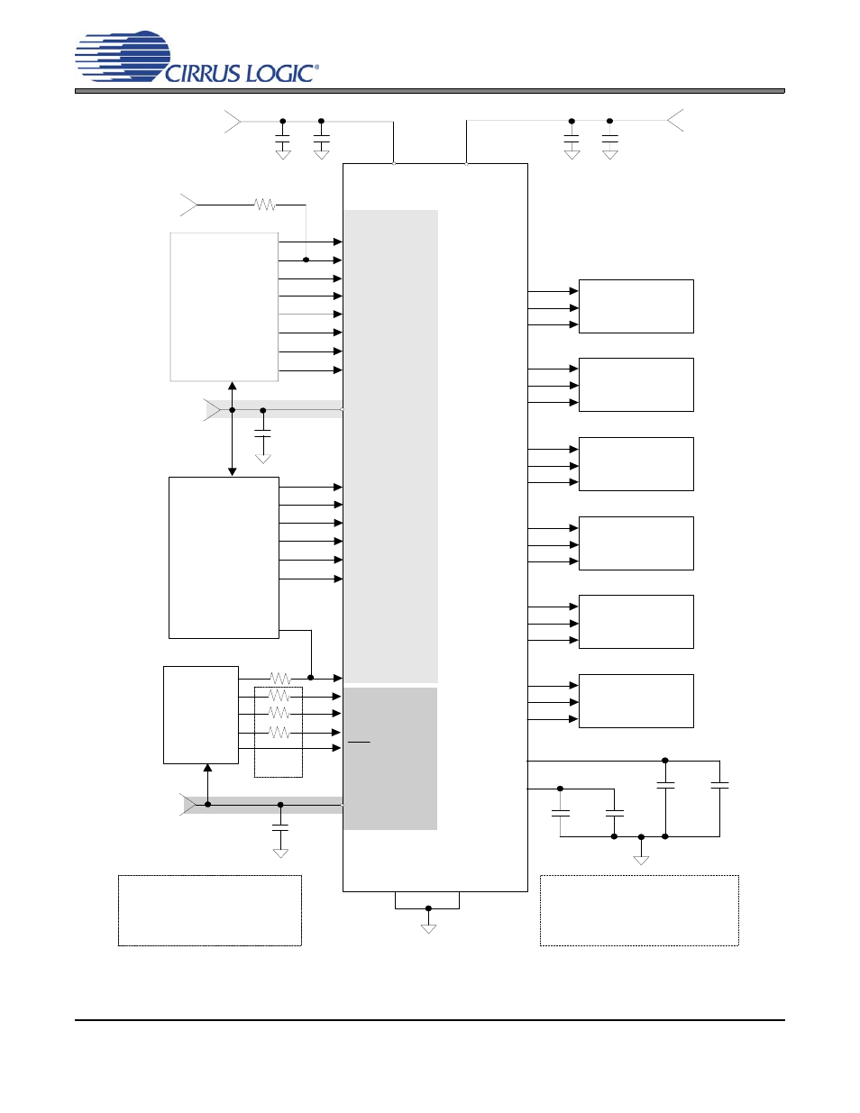
Figure 6. typical connection diagram stand-alone, Cs4362, C s 4362 – Cirrus Logic CS4362 User Manual
Page 14
14
DS257F2
CS4362
D igital
Audio
S ource
V LS
C S 4362
M C LK
VD
A O U TA 1+
10
8
32
0.1 µF
+
1 µF
+3.3 V to +5 V
S DIN 1
9
1 µF
0.1 µ F
+
+
20
21
FILT+
C M O UT
7
6
LR C K 1
S CLK1
S DIN 3
S DIN 2
39
40
0.1 µ F
47 µF
VA
0.1 µF
+
1 µF
0.1 µF
+1.8 V to +5 V
+5 V
4
43
LR C K 2
S CLK2
13
A O UTA1-
A O U TB 1+
38
37
A O UTB1-
A O U TA 2+
35
36
A O UTA2-
A O U TB 2+
34
33
A O UTB2-
A O U TA 3+
29
30
A O UTA3-
A O U TB 3+
28
27
Analog Conditioning
and M uting
A O UTB3-
11
12
P CM
31
G ND
G N D
5
V LC
0.1 µF
+1.8 V to +5 V
18
D S D
A udio
Source
2
48
DS D B2
3
42
M3(DS D _SC LK )
DS D A1
D S DB 3
D S DA 3
DS D B1
D S DA 2
46
47
1
16
15
M 2
M 1
M 0
RS T
19
17
47 K
Ω
VLS
N ote
D SD
Note
DSD
N ote
D SD
: For D S D operation:
1) LR CK 1 m ust be tied to V LS and
rem ain static high.
2) M 3 PC M stand-alone configuration
pin becom es DS D _SC LK
22
M U TEC 6
Analog Conditioning
and M uting
23
M U TEC 5
Analog Conditioning
and M uting
24
M UTEC 4
Analog Conditioning
and M uting
25
M UTEC 3
Analog Conditioning
and M uting
26
M UTEC 2
Analog Conditioning
and M uting
41
M UTEC 1
S tand-A lone
Mode
C onfiguration
47 K
Ω
N ote
VLC
Note
VLC
: If series resistors are
used they m ust be <1k O hm . If
possible tie V LC to the V D supply
to reduce possible excess current
consum ption from V LC .
Figure 6. Typical Connection Diagram Stand-Alone