Cirrus Logic CS4362 User Manual
Cs4362, Features, Description
Copyright
© Cirrus Logic, Inc. 2008
(All Rights Reserved)
114 dB, 192 kHz 6-Channel D/A Converter
Features
24-bit Conversion
Up to 192 kHz Sample Rates
114 dB Dynamic Range
-100 dB THD+N
Supports PCM or DSD Data Formats
Selectable Digital Filters
Volume Control with Soft Ramp
–
1 dB Step Size
–
Zero Crossing Click-free Transitions
Dedicated DSD Inputs
Low Clock Jitter Sensitivity
Simultaneous Support for Two Synchronous
Sample Rates for DVD Audio
μC or Stand-Alone Operation
Description
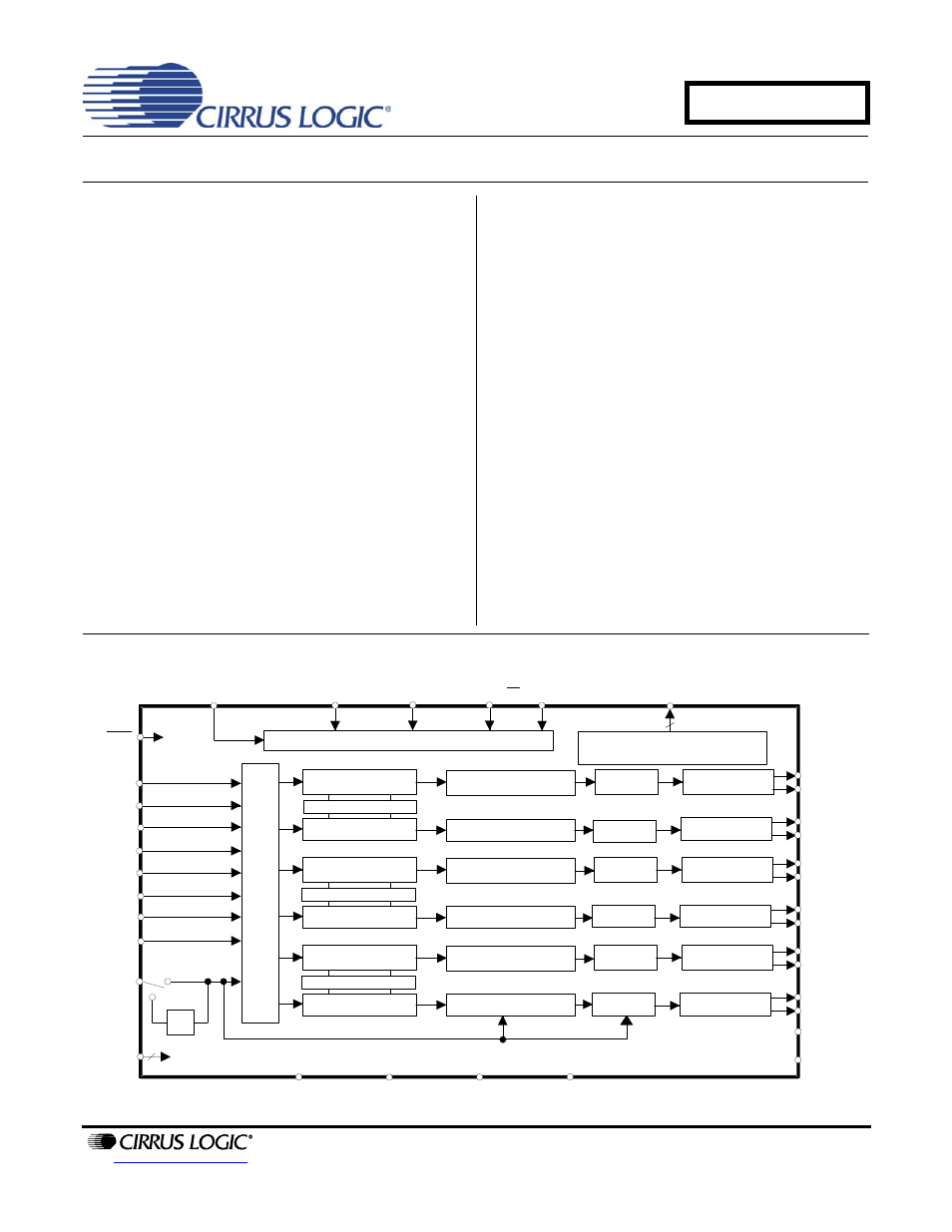
The CS4362 is a complete 6-channel digital-to-analog
system including digital interpolation, fifth-order delta-
sigma digital-to-analog conversion, digital de-empha-
sis, volume control and analog filtering. The advantages
of this architecture include: ideal differential linearity, no
distortion mechanisms due to resistor matching errors,
no linearity drift over time and temperature and a high
tolerance to clock jitter.
The CS4362 is available in a 48-pin LQFP package in
Commercial grade (-10°C to +70°C). The CDB4362
Customer Demonstration Board is also available for de-
vice evaluation and implementation suggestions.
Please see
“Ordering Information” on page 42
plete details.
The CS4362 accepts PCM data at sample rates from
4 kHz to 192 kHz, DSD audio data, and operates over a
wide power supply range. These features are ideal for
multi-channel audio systems including DVD players.
SACD players, A/V receivers, digital TV’s, mixing con-
soles, and effects processors.
I
E x t e r n a l
M u t e C o n t r o l
R S T
V o l u m e C o n t r o l
I n t e r p o l a t i o n F i lt e r
A n a l o g F i lt e r
Δ Σ
D A C
M i x e r
V o l u m e C o n t r o l
Δ Σ
D A C
A n a l o g F i lt e r
I n t e r p o l a t i o n F i lt e r
V o l u m e C o n t r o l
I n t e r p o l a t i o n F i lt e r
A n a l o g F i lt e r
Δ Σ
D A C
M i x e r
V o l u m e C o n t r o l
Δ Σ
D A C
A n a l o g F i lt e r
I n t e r p o l a t i o n F i lt e r
V o l u m e C o n t r o l
I n t e r p o l a t i o n F i lt e r
A n a l o g F i lt e r
Δ Σ
D A C
M i x e r
V o l u m e C o n t r o l
Δ Σ
D A C
A n a l o g F i lt e r
A O U T B3-
I n t e r p o l a t i o n F i lt e r
M C L K
Ser
ia
l
P
o
rt
M 1/SCL/CCLK
M 2/SDA/CDIN
M 0/AD0/CS
VLC
÷
2
VQ
FILT+
VA
GND
VD
M UTEC[1:6]
M 3/DSD_SCLK
G ND
Control Port/M ode Select
6
VLS
L R C K
S D I N 1
S D I N 2
S D I N 3
2
S C L K
L R C K 2
S C L K
DSDxx
6
A O U T B3+
A O U T A3-
A O U T A3+
A O U T B2-
A O U T B2+
A O U T A2-
A O U T A2+
A O U T B1-
A O U T B1+
A O U T A1-
A O U T A1+
1
1
FEB '08
DS257F2
CS4362
Document Outline
- 1. Characteristics and Specifications
- Analog Characteristics
- Analog Characteristics
- Power and Thermal Characteristics
- Analog Filter Response
- Digital Characteristics
- Absolute Maximum Ratings
- Recommended Operating Conditions
- Switching Characteristics
- DSD - Switching Characteristics
- Switching Characteristics - Control Port - I·C® Format
- Switching Characteristics - Control Port - SPI™ Format
- 2. Typical Connection Diagram
- 3. Register Quick Reference
- 4. Register Description
- 4.1 Mode Control 1 (address 01h)
- 4.2 Mode Control 2 (address 02h)
- 4.3 Mode Control 3 (address 03h)
- 4.4 Filter Control (address 04h)
- 4.5 Invert Control (address 05h)
- 4.6 Mixing Control Pair 1 (Channels A1 & B1)(address 06h) Mixing Control Pair 2 (Channels A2 & B2...
- 4.7 Volume Control (addresses 07h, 08h, 0Ah, 0Bh, 0Dh, 0Eh)
- 4.8 Chip Revision (address 12h)
- 5. Pin Description
- 6. Applications
- 7. Control Port Interface
- 8. Filter Plots
- Figure 9. Single-Speed (fast) Stopband Rejection
- Figure 10. Single-Speed (fast) Transition Band
- Figure 11. Single-Speed (fast) Transition Band (detail)
- Figure 12. Single-Speed (fast) Passband Ripple
- Figure 13. Single-Speed (slow) Stopband Rejection
- Figure 14. Single-Speed (slow) Transition Band
- Figure 15. Single-Speed (slow) Transition Band (detail)
- Figure 16. Single-Speed (slow) Passband Ripple
- Figure 17. Double-Speed (fast) Stopband Rejection
- Figure 18. Double-Speed (fast) Transition Band
- Figure 19. Double-Speed (fast) Transition Band (detail)
- Figure 20. Double-Speed (fast) Passband Ripple
- Figure 21. Double-Speed (slow) Stopband Rejection
- Figure 22. Double-Speed (slow) Transition Band
- Figure 23. Double-Speed (slow) Transition Band (detail)
- Figure 24. Double-Speed (slow) Passband Ripple
- Figure 25. Quad-Speed (fast) Stopband Rejection
- Figure 26. Quad-Speed (fast) Transition Band
- Figure 27. Quad-Speed (fast) Transition Band
- Figure 28. Quad-Speed (fast) Passband Ripple
- Figure 29. Quad-Speed (slow) Stopband Rejection
- Figure 30. Quad-Speed (slow) Transition Band
- Figure 31. Quad-Speed (slow) Transition Band (detail)
- Figure 32. Quad-Speed (slow) Passband Ripple
- 9. Diagrams
- Figure 33. Format 0 - Left Justified up to 24-bit Data
- Figure 34. Format 1 - I·S up to 24-bit Data
- Figure 35. Format 2 - Right Justified 16-bit Data
- Figure 36. Format 3 - Right Justified 24-bit Data
- Figure 37. Format 4 - Right Justified 20-bit Data
- Figure 38. Format 5 - Right Justified 18-bit Data
- Figure 39. De-Emphasis Curve
- Figure 40. Channel Pair Routing Diagram (x = Channel Pair 1, 2, or 3)
- Figure 41. ATAPI Block Diagram (x = channel pair 1, 2, or 3)
- Figure 42. Recommended Output Filter
- 10. Parameter Definitions
- 11. References
- 12. Package Dimensions
- 13. Ordering Information
- 14. Revision History